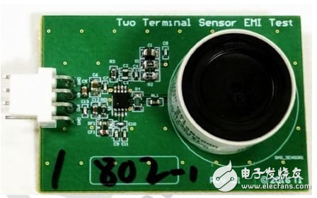
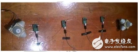
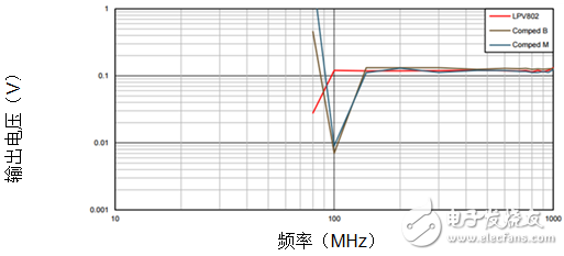
Designers of Internet of Things (IoT) applications focus on two things: managing power supplies to maximize battery life, ensuring reliable operation and preventing electromagnetic interference (EMI). The IoT revolution will lead the way in billions of battery and line-powered connected devices, including many wireless devices. All of these devices are competing for the same frequency spectrum. This will create an increasingly noisy environment in which electromagnetic waves generate radiation from multiple sources. Since the introduction of wireless devices, electromagnetic signal interference has become a problem in sharing unlicensed spectrum, and as the number of devices in operation increases, the importance of the problem increases. Wireless-capable terminal devices such as smoke detectors, toxic gas sensors, and PIR sensors require additional radiated EMI testing due to their interaction, as shown in Figure 1. Figure 1: Passive Infrared (PIR) Sensor with Electromagnetic Wave and Carbon Monoxide Detector The competition to create wireless sensing nodes brings a degree of complexity to EMI testing. System designers need to carefully select components to avoid the costly redesign, as this may delay time to market in the final stages of product development. In addition to operating under noisy conditions, battery-powered connected devices need to operate safely and reliably for years without replacing the battery. The battery life of IoT devices varies widely, from hours to years, depending on the application and its operating environment. Designers of these IoT devices must select components with very low current consumption to extend operating life and provide EMI immunity. TI's LPV811 series of nanopower amplifiers consume quiescent currents as low as 320nA to maximize battery life and protect them from EMI. However, these devices do not include the full input EMI filter seen on many recently released operational amplifiers. We do this for a reason, because adding an input EMI filter greatly increases the input capacitance, which can result in peaks in sub-micron circuits with large feedback resistance values ​​and source impedance. Instead, we used internal (proprietary) precautions in the layout and internal design of the LPV801, LPV802, LPV811, and LPV812 to make them as resistant as possible to EMI. To validate the effectiveness of our built-in EMI mitigation technology, we compared the LPV 802 and two other similar devices in the market that do not have internal EMI protection. In all environments, circuits using the LPV 802 exhibit better EMI immunity than circuits using similar devices. We tested the EMI tolerance of all three devices according to IEC 61000-4-3 (Electromagnetic Compatibility (EMC) - Radiation Test Conditions). We place the device under test (DUT) in the calibrated radio frequency (RF) range from 80MHz to 6GHz while monitoring the DUT's fault according to the IEC 61000-4-3 EMC emission specification. To compare the three devices, we simultaneously exposed the three devices to the same EMC radiation in the same circuit and monitored their output deviation. In addition, to measure the effectiveness of common EMI filtering techniques, we tested two sets of boards. One set of boards adds external input EMI capacitors, and the other set of boards does not have EMI capacitors. Figure 2 shows a test board built on a standard 62 mil, dual-layer FR4 board with ground planes on both sides to test EMI performance. The four-pin connector allows quick replacement of the board. Plugging the sensor pins makes it easier to remove the sensor. Figure 2: Test board with sensor Figure 3 shows the test setup. There are four test boards to test EMI performance. The three test boards have the same circuit with different operational amplifiers mounted on them. Another test board was built with a ground reference configuration but was not used in the test. We connected each of the four test boards to a central battery box (2 AA batteries) via a 1 m long four-conductor shielded cable with EMI chokes at both ends. We connected the battery compartment to the control room via a 15-meter long UTP CAT-5 cable and used an appropriate EMI choke to supply the output voltage to the recording system. Two white boxes with cones are field sensors for monitoring the electric field during the test. Figure 3: Test setup for IEC61000-4-3 EMC radiation test Figure 4 shows one of the test results specified in IEC 61000-4-3. At the 30V / m radiation level, two similar devices begin to weaken at 140MHz, while the LPV802 remains at 100MHz. In general, circuits using the LPV802 have better EMI performance than circuits using similar devices of the same brand, and are tested in all specified tests for different levels of radiation, especially in the 100-200 MHz range. Most devices are not affected by the upper frequency ("400MHz). For more information on test conditions and results, see the application note "Comparing EMI Performance of LPV802 with Other Devices in Gas Sensor Applications." Figure 4: Results of a 30V / m test using a capacitor Adding an external EMI input capacitor also contributes to overall performance. We recommend adding it during the normal design process. EMI protection does not completely eliminate the effects of EMI, but it does help to reduce the impact. Adding an external filter can further reduce the impact. Even with EMI-protected equipment, we recommend external filtering. Using components such as LPV801, LPV802, LPV811, and LPV812 that consume nanoamperes of quiescent current and immunity to EMI can help designers build systems with longer battery life and global EMI regulations. This helps reduce maintenance costs and speed time to market. There is no need to worry about EMI failures in the final stages of product development and costly redesigns. Solder Cup Waterproof D-Sub Connector
The Solder Cups D-sub connector, also known as Solder Cups D-sub connector , typically contains a pin layout of 9 pin, 15 pin, 25 pin, 37 pin & 50 pin positions housed in increasing shell sizes accordingly. They are available in both male (plug) and female (socket) variants with the male signal contacts/pins (current rating of 5A) spaced every 2.76mm in horizontal rows and the spacing of rows vertically at 2.84mm laid out half the distance between pins of existing rows.
IP66 IP67 Rated Waterproof D-Sub Panel Mount Solder Connectors
Antenk offer a wide range of waterproof standard density and high density male and female high density D-Sub connectors solder cup with stamped and formed Contacts in cable mount used in a variety of demanding applications.
Antenk's Solder Cup D-Sub Connectors Stamped contacts
FEATURES
Solder cup d-subs available in industry sizes/positions
Low cost economy series.
Nickel shells have indents to provide grounding and additional retention.
Low cost & high performance, non-removable stamped contacts.
Optional mounting hardware available.
Antenk's SOLDER CUP D-SUB CONNECTORS Stamped contacts
MATERIALS
Shell: Steel, Tin or Nickel Plated
Insulator: Glass-filled thermoplastic. U.L. rated 94V-O
(230°C process temp)
Stamped contacts: Male pins - Brass | Female pins - Phosphor bronze
Plating: Gold flash on entire contact (contact us for other plating options)
Solder Cup Waterproof D-Sub Connector Stamped & Formed Contact, Solder Cup Waterproof D-Sub Connector Machined Contacts, Waterproof Panel Mount Solder Cup D-Sub Connector ShenZhen Antenk Electronics Co,Ltd , https://www.antenkelec.com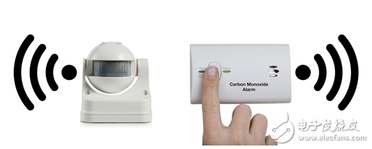
Harsh outdoor or indoor environments can destroy electronic equipment. Standard D-sub connectors are not intended to withstand contaminants such as water and dust. These waterproof solder cup connectors are available in male or female genders and DB9, DB15, DB25, and HD15 sizes. They will accommodate wire ranges from 30 - 20 AWG. Construction features gold plated brass contacts, nickel plated steel shells, and a silicone insulating ring. Maximum recommended panel thickness is 0.078".