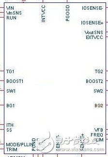
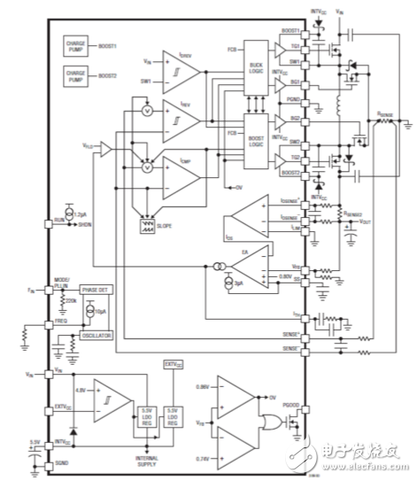
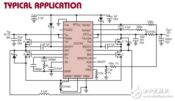
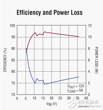
In buck or boost mode, the LTC3789 uses a proprietary current mode control architecture for constant frequency operation with four powerful N-channel MOSFET gate drivers. The LTC3789 also provides an accurate constant current regulation loop to regulate the input or output current over a wide input voltage range. The input current limit feature prevents input supply overload and the output current limit provides an easy solution for stable output current applications such as battery chargers or LED drivers. The device provides fault protection for overvoltage, overcurrent, and short-circuit conditions in all operating modes. In addition, the LTC3789 disconnects the input voltage and output voltage during shutdown. The user can select either continuous or pulse skip mode to maximize light load efficiency and allow the IC to be synchronized to an external clock. The pulse skip mode achieves the lowest ripple under light load conditions, while the forced continuous mode operates at a constant frequency to meet the needs of noise sensitive applications. In addition, the LTC3789 features an adjustable soft-start, power-good output and ±1.5% reference accuracy over the operating junction temperature range of -40°C to 125°C. 1. VFB (PIN1/PIN26): Error amplifier feedback pin. The feedback voltage received by the LTC3789 is derived from the voltage output from the external resistor divider. 2. SS (PIN2/PIN27): External soft start input pin. The LTC3789 regulates the VFB voltage to a small 0.8V or SS pin. A 3μA internal pullup current source is connected to this pin. Connect a capacitor to this pin to ground to set the slope of the rise of the final output stable voltage. 3. SENSE+ (PIN3/PIN28): Current sense comparator non-inverting input. The ITH pin voltage and the offset voltage between SENSE- and SENSE+ are combined with the current sense resistor RSENSE to set the current threshold. 4. SENSE-(PIN4/PIN1): Current detection comparator inverting input. 5. ITH (PIN5/PIN2): Error amplifier output and switching regulator compensation point. This channel current comparator threshold point increases as the voltage at this pin increases. 6. SGND (PIN6/PINS3, EXPOSED PAD PIN29): Small signal ground. This pin must be wired separately to the common terminal of the negative current of the input filter capacitor CIN. In the QFN package, the exposed pad is SGND. For rated thermal performance, it must be soldered to the ground of the PCB. 7. MODE/PLLIN (PIN7/PIN4): Mode selection or external sync input to the phase detector. This is a dual purpose pin. This pin selects the operating mode when external frequency synchronization is not available. This pin can be tied to SGND or INTVCC. Forced continuous mode is enabled when connected to SGND or below 0.8V. Connect to INTVCC enable pulse skip mode. For external sync mode, the clock signal is applied to this pin. The internal PLL will synchronize the internal oscillator's clock and the forced continuous mode will be enabled. A network of PLLs has been integrated into the IC. 8. FREQ (PIN8/PIN5): Frequency setting pin. There is a precise 10uA current flowing from this pin. A voltage is set by a grounding resistor to change the frequency. In addition, this pin can be driven with a DC voltage to change the frequency of the internal oscillator. 9. RUN (PIN9/PIN6): Run the control pin. When this pin is below 0.5V, the controller will be turned off and the quiescent current will be reduced. This pin has a 1.2uA pull-up current. Once this pin voltage is above 1.22V, the IC is turned on and a 5uA pull-up current is added to this pin. 10. VINSNS (PIN10/PIN7): The buck-boost conversion compare pin for the VIN sense input. This pin is connected to the drain input of the uppermost N-channel MOSFET. 11. VOUTSNS (PIN11/PIN8): VOUT sense input buck-boost conversion compare pin. This pin is connected to the drain output of the uppermost N-channel MOSFET. 12. ILIM (PIN12/PIN9): Input/output average current detection range input pin. This pin is tied to SGND, INTVCC or floating to set the maximum average current detection threshold. 13. IOSENSE+(PIN13/PIN10): input and output average current sense amplifier non-inverting input terminal 14. IOSENSE-(PIN14/PIN11): input and output average current sense amplifier inverting input terminal 15. TRIM (PIN15/PIN12): For normal chip operation, connect this pin to GND. This pin is not allowed to float. 16. EXTVCC (PIN20/PIN17): The external power input is connected to INTVCC via an internal LDO. The LDO provides an INTVCC supply that bypasses the internal LDO and then VIN when EXTVCC is above 4.8V. Check the EXTVCC pin connection in the Application Information section. This pin voltage cannot exceed 14V. 17. INTVCC (PIN21/PIN18): Output of the internal LDO. This drive and control circuit is powered from a voltage source. This pin must use a minimum of 4.7uF tantalum capacitor, ceramic or other low ESR capacitor. 18. Vin (PIN22/PIN19): Main power input pin. A bypass capacitor should be connected between this pin and the signal ground pin. 19. BG1, BG2 (PINS 23, 19/PINS 20, 16): High current gate driver for the bottom (synchronous) N-channel MOSFET. The voltage swing at these pins is from the power ground to INTVCC. 20. PGND (PIN24/PIN21): Drive power ground. Connect to the end of COUT and CIN, the negative side of the RSENSE resistor. 21. BOOST1, BOOST2 (PINS 25, 18/PINS 22, 15): Bootstrap power supply for the top floating drive. On the BOOST pin and SW Connect a capacitor between the pins and connect a Schottky diode between the BOOST pin and INTVCC. The voltage swing on the BOOST1 pin ranges from INTVCC to (VIN + INTVCC). The voltage swing on the BOOST2 pin ranges from INTVCC to (VOUT + INTVCC). 22. TG1, TG2 (PIN 26, 17/PIN 23, 14): High current gate driver for the front N-channel MOSFET. These floating drive output voltage swings are equal to INTVCC - 0.5V superimposed on the SW1 pin (or SW2 pin) switch node voltage. 23. SW1, SW2 (PINS 27, 16/PINS 24, 13): A switching node connected to the inductor. The voltage swing on the SW1 pin is the voltage drop from a Schottky diode (external) below ground to VIN, and the voltage swing at the SW2 pin is from a Schottky diode below ground. The voltage drop to VOUT. 24. PGOOD (PIN 28/PIN 25): Logic output (open drain mode). When the internal 20us POWER-BAD time stamp timer expires, PGOOD will be connected to ground when the voltage on the VFB pin is not within ±10% of its adjustment window. Internal equivalent circuit of LTC3789 The LTC3789 is a current mode controller. It provides an output voltage that can be higher or lower than the input voltage, LTC proprietary topology and control method. Using a current sense resistor, the inductor current is controlled by the voltage on the ITH terminal, which is the output of the error amplifier EA. The VFB terminal receives the feedback voltage signal, which is compared to the internal reference voltage applied to the EA. If the input and output current regulation loops are Execution, the detected inductor current is controlled by the feedback voltage or the current flowing in and out. Single inductor architecture Operates with an input voltage higher than, lower than or equal to the output voltage 4V to 38V input voltage range 0.8V to 38V output voltage range Programmable input or output current limit Synchronous rectification Up to 98% efficiency Built-in MOSFET gate driver Can provide 150W output power Output disconnection when shutdown PLL fixed operating frequency from 200kHz to 600kHz Power good output signal ±1.5% reference voltage accuracy over the -40oC to +125oC temperature range Current mode control for fast transient response and very easy loop compensation Overvoltage and overcurrent protection 5.5V internal and external VCC LDO
High efficient charging speed for Lenovo and IBM laptop, stable current outlet can offer power for the laptop at the same time charge the laptop battery. The best choice for your replacement adapter. We can meet your specific requirement of the products, like label design. The plug type is US/UK/AU/EU.The material of these products is PC+ABS. All condition of our products is 100% brand new.
Our products built with input/output overvoltage protection, input/output overcurrent protection, over temperature protection, over power protection and short circuit protection. You can send more details of this product, so that we can offer best service to you!
Lenovo Adapter,Charger For Lenovo,Power Supply For Lenovo,Adapter For Lenovo Mini Shenzhen Waweis Technology Co., Ltd. , https://www.szwaweischarger.com


The LTC3789 is a high performance, buck-boost switching regulator controller that operates with input voltages above, below or equal to the output voltage. The device utilizes a constant frequency, current mode architecture to provide a phase-lockable frequency of up to 600kHz, while an output current feedback loop provides support for battery charging. With a wide input and output range of 4V to 38V (40V maximum) and seamless and low noise conversion between workspaces, the LTC3789 is ideal for automotive, telecom and battery-powered systems.
When the output is within 10% of its design set point, an indication signal will be generated on a power good output pin. The LTC3789 is available in a low profile 28-pin 4mm x 5mm QFN package and a narrow body SSOP package.
LTC3789 pin description LTC3789 pin diagram