planar magnetics transformer,High Frequency T 200W Planar Transformer,flyback planar transformer,coilcraft planar transformer IHUA INDUSTRIES CO.,LTD. , https://www.ihua-coil.com
The MAX3250 high-offset-voltage (high-VOS) rejecTIon RS-232 transceiver provides a ± 50V isolated data interface and power for the line-side transceiver circuits. Unlike opTIcally- or transformer-isolated RS-232 transceivers, its main features are low cost, an allowed ± 50V resisTIve-isolation character in a single small IC package, and capacitive power transfer from non-isolated to isolated-side circuitry. It operates from a single +3.3 or + 5V system-power source, and requires only external surface-mount capacitors for operation. An overall low profile is maintained when compared to other isolation techniques requiring opto-couplers and / or a transformer.
This paper describes how resistor-isolated transceivers are able to handle ± 50V ground-offset signals, and indicates how and why the offset voltage is limited by the design. The method of transferring power across the isolation barrier is explained. Pseudo-Isolated RS- 232 TransceiverThe MAX3250 provides a ± 50V isolated data interface while, in the same IC package, providing isolated power for the line-side transceiver circuits from a single +3 to + 5.5V system power source. The detailed functional diagram in Figure 1 allows a clear visualization of the isolation, power-transfer, and protection circuits. External filter, charge-pump, and power-transfer capacitors are utilized. 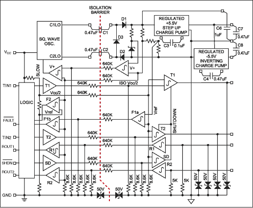
Figure 1. MAX3250 functional block diagram.
When RS-232 cables connect between buildings, the originating signal common or ground may not be at the same electrical potential as that of the receiving-location ground. Typically, the drive-circuit common is connected to chassis or frame ground either directly or through a 100Ω resistor. Hence, the situation illustrated graphically in Figure 2 may exist. 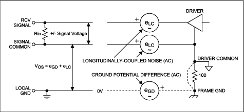
Figure 2. Offset voltages in two-wire line data-transmission system.
The ISO COM and the data line will take on an offset voltage equal to the vector sum of the ground-potential difference and any longitudinally-coupled noise voltage generated along the signal path between transmitter and receiver.  The receiving-location ground potential may differ substantially from the potential at the driver-location, and it is the difference between the two that is of interest when considering application of the MAX3250. This offset voltage (VOS) must be isolated from the logic side of the MAX3250. How High-Offset-Voltage Transceivers WorkHigh-VOS data transceivers include no truly isolated circuits. Instead, they separate logic-side circuitry from line-side circuitry with high-value resistive attenuators as detailed in Figure 3. These attenuators are Typically constructed so that about 1% of the input signal reaches the attenuator output. Consequently, only 1% of the applied isolation voltage reaches across the resistive barrier. Separate drivers send data across the barrier in each direction where the signal is attenuated before being detected by comparators on each side of the barrier. Attenuators in the MAX3250 have a ratio of 75: 1.
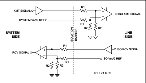
Figure 3. Resistive isolation technique.
Reference voltages are also created on each side and sent across the barrier with identical 75: 1 attenuation to bias the receiving comparators which then see the same common-mode offset voltage on both signal and reference lines. As the comparators read both the attenuated signal and the attenuated reference, an offset voltage of 50V occurring on the line would only translate to a 2 / 3V common-mode voltage on the outputs of the resistive barriers. As long as the differential receiver can accept the 2 / 3V CM voltage and is sensitive enough to detect 1 / 75th of the differential-signal input to the resistive attenuator, the system will operate correctly.
Thus, a full bi-directional signaling system is created with 75: 1 barrier attenuation of all signals to allow two-way communication and a 50V difference across the resistive barrier. This is a pseudo-isolated circuit rather than a classically isolated circuit, yet it accomplishes the isolation needed in perhaps the majority of applications.
Note that there is a resistance between ISO COM and system GND (see Figure 1) due to the existence of nine sets of isolation resistors. The approximate parallel resistance of these nine attenuators is 72kΩ. Power Transfer Across the Isolation BarrierUnless a separate isolated power supply is available to operate the isolated RS-232 transceiver, power must be transmitted from the system or non-isolated side to the line or isolated-side circuits without destroying the required isolation. It is a practical matter to use capacitive voltage transfer across the isolation barrier when the planned isolation is no more than 50-100V. Higher voltages can be isolated; but the required capacitors become somewhat large at, say, 500V. Capacitive power transfer can be accomplished by differentially driving a pair of capacitors from a square-wave oscillator on the system side as indicated in Figure 4. The external capacitors feed three diodes and a filter capacitor on the isolated side to produce an i solated DC output. The third diode is present to allow recharging / discharging of the coupling capacitors on alternate half-cycles of the oscillator signal. The coupling-capacitor voltage ratings are selected to be greater than the required line-side isolation or offset voltage. 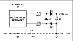
Figure 4. Capacitor-coupled isolated supply.
The isolated-supply power-transfer system operates somewhat like the well-known charge pump. The square-wave oscillator reverses its output polarity (0 or + 5V) on alternate half cycles of operation. Its output is always a square wave (50% duty cycle), but (in the MAX3250) its output resistance increases on command (via a return feedback path visible in Figure 1) when ISO VCC reaches its design voltage. Thus, it operates to provide either normal or reduced power transfer to the isolated supply. As the line-side load draws down the voltage on C6, the feed-back signal will again cause the oscillator to more effectively replenish the charge on C6. The output voltage is thus under active regulation, with some ripple on the output at a ripple frequency depending upon the actual load. A Zener diode on the output side acts as a voltage reference against which a fraction of the output is compared to drive the control signal that is sent back across the isolation barrier to the oscillator. The c harge pump injects noise currents into the ISO COM terminal to create a noise voltage on ISO COM whenever ISO COM is not connected to system GND. Hence, ISO COM should be bypassed to system GND with a 10nF capacitor (C9 in Figure 4). There are two additional regulating charge pumps driven by ISO VCC to create regulated ± 5.5V supplies for the RS-232 drivers and receivers. Control and Data Transfer Across the Isolation Barrier (refer to Figure 1) Isolation is provided by the resistive isolation technique already described . Note that the shut-down (SHDN) and both transmit (TIN) signals cross the isolation barrier from left to right or from the logic side to the line side as signals referenced to a logic-side reference voltage. The two received-data (RIN) signals cross the isolation barrier from right to left or from line side to logic side as a signal referenced to a line-side reference voltage. All signals, including references, are attenuated after crossing the isolation barrier by an i dentical amount of 1/75 or 1.33% of signal. Each attenuated data or control signal is applied to one comparator input, and the associated attenuated reference voltage is applied to the other comparator input. The reference voltages are designed to be midway between the high and low levels of the data and control signals so that each comparator operates at maximum sensitivity.
Two more signals cross the isolation barrier from right to left. These are the previously-discussed control signal to inform the logic-side circuits that the isolated supply voltage is at its design level and a fault signal to inform a connected processor when the ± 50V isolation voltage limits are exceeded. Line-Interface Driver and Receiver CircuitryTypical connection between an RS-232 transceiver and the two-wire data line is illustrated in Figure 5 (transmit and additional receive lines are omitted for clarity). The cable is not terminated except by the receiver's internal resistance (RIN = 5kΩ). The cable could be shielded with the shield connected to the frame ground as shown. The shield should not be grounded at both ends, otherwise a current may be set up in the shield due to any ground-offset voltage. Any longitudinally-coupled noise signal is probably insignificant or absent when the line is shielded. The offset voltage, VOS, appears equally on the data and return lines wher e it is seen as a common-mode voltage in relation to GND. The VOS is applied directly to ISO COM via the data common line and to RIN via the received-data line. 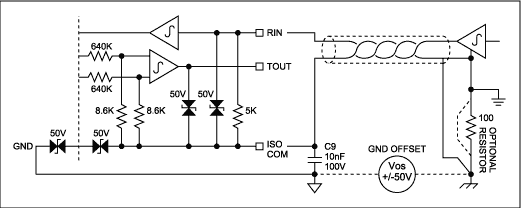
Figure 5. MAX3250 line interface circuitry with shielded line.
The RS-232 standard defines a minimum ± 5V transmitted signal level, a maximum ± 3V receiver detection level, and a 3-7kΩ receiver input resistance measured from receiver input to signal common (ISO COM in this example). The MAX3250 receiver-input -threshold worst-case specifications are VIL ≥ 0.6V and VIH ≤ 2.4V. However, actual guarded distribution over the specified supply voltage and temperature range is VIL ≥ 1.0V and VIH ≤ 2.0V. Receiver noise margins are [VIL-(- 5V)] ≥ 6V at the low end and [5V-VIH] ≥ 3V at the high end, easily falling within the standard RS232-compliant range, and are satisfactory even in an RS232-compatible system. Offset-Voltage Noise ConsiderationsThe AC offset voltage is of power-line frequency plus primarily 2nd and 3rd harmonics although some higher-order harmonics may be present. The isolation noise signal does not appear across the receiver-input resistors because this noise is a common-mode signal appearing equally (with respect to GND) o n both receiver input and common lines. The only noise signal that might appear across the receiver-input resistors is an unbalanced portion of any conducted or longitudinally-coupled noise rising unequally on the receiver input and common lines. Figure 6 shows an example of conducted noise produced by RS-232 transmitter signals. In this example, two ± 6V transmitted signals applied to remote receivers ?? Ewith the minimum 3kΩ receiver input resistance allowed by the RS-232 specification ?? Ecreate a ± 4mA transmitter signal current flowing in the data common line. Allowing for the RS-232 specified maximum cable resistance of 25Ω (half in the common line), an interfering signal of ± 50mV (4mA × 12.5Ω) appears effectively in series with the received data signal. Even with these worst -case resistance values, the conducted noise is well within the receiver noise margins. Unbalanced longitudinally-coupled noises are not considered as they are likely to be insignificant when twisted-pair lines are utilized. 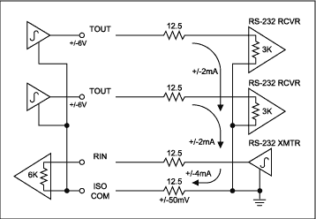
Figure 6. Conducted noise example. Offset Isolation-Voltage Limits The isolation voltage limits of the MAX3250 are determined by two characteristics.
1. The charge-pump isolation-voltage limit is set by the breakdown rating of capacitors C1, C2, and C9 (see Figure 4).
2. The data-transfer-circuitry isolation-voltage limit is set by a combination of the resistive-attenuator ratio, driver-signaling levels (related to the non-isolated and the isolated-supply voltages), differential-comparator common-mode range , and comparator signal-discrimination characteristics in the presence of noise. The specified limit for the MAX3250 is ± 50V with an absolute maximum rating of ± 80V. Internal back-to-back SCRs between logic and line circuits will break down when the limits are exceeded. Offset Isolation-Voltage and Frequency ConsiderationsThe maximum applied offset voltage is dependent on frequency and the value of the power coupling capacitors (C1 and C2 in Figures 1 and 4). The dependence on C1 and C2 is due to a reverse pumping action caused by high levels of ground offset voltage. This means that there are different limits to VOS when the circuit is powered by 3.3V or 5V supplies because C1 and C2 must be 470nF for 3.3V supply whereas 47nF is allowed for a 5 V supply.
The isolated supply of Figure 4 is redrawn in Figure 7 to include details of the square-pulse oscillator. Reverse charging paths are shown for VOS-generated currents. When the VOS polarity is as shown, a current, indicated by the solid line, will flow through Q2, C1, and D1 to charge C6. When the polarity is reversed, a current, indicated by the dashed line, will flow through D2, C2, and Q3 to charge logic-bypass capacitor C5. 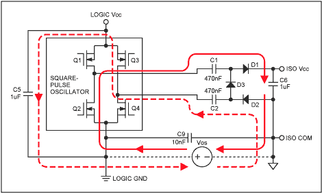
Figure 7. Equivalent charge transfer circuit showing possible reverse pumping paths for Vos.
The result of these reverse pump currents is insignificant for 5V logic operation when C1 and C2 are 47nF. No practical effect is seen for VOS = ± 50V even at 600Hz. A small ripple voltage may be observed on C6 at the higher frequencies. This is indicated by the flat curve in Figure 8 for 5V operation.
The results, however, are not insignificant for 3.3V operation when C1 and C2 are 470nF. As frequency and voltage are increased, ripple becomes increasingly apparent on C6. Eventually, ISO V + is also affected. In extreme cases, ripple may begin to show on the logic supply at C5. The curve for 3.3V operation in Figure 8 indicates the maximum applied isolation voltage vs. frequency for a 100ns jitter in received pulse width. This occurs when the modulation on C6 approaches 3Vpp. The maximum applied VOS is ± 50V at or below 80Hz, and decreases with frequency as shown. The curve will vary slightly with tolerance and temperature variations in the values ​​of C1, C2, and C6 so this must be considered as a typical curve. Still, rather high levels of power -line harmonics can be tolerated. 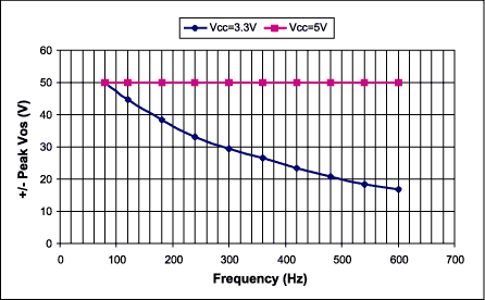
Figure 8. Maximum applied offset voltage vs. frequency for 3.3V and 5V operation.
The capacitors selected for C1, C2, and C9 should be rated for 100V operation. Suitable surface-mount capacitors are: MuRata
GRM40X7R103K100 (10nF, 0805)
GRM43X7R473K100 (47nF, 1808), and
GRM44-1X7R474K100 (470nF, 2220), or equivalents.
Suitable radial-lead metalized film capacitors are: ITW Paktron
103K250RA2 (10nF, 250VDC)
473K100RA2 (47nF, 100VDC), and
474K100RA2 (470nF, 100VDC), or equivalents. Fail SafeThe RS-232 specification defines receiver differential thresholds as + 3V and –3V. However, when a two-wire line is open circuited or when the line driver is not powered, the receive line signal voltage will be 0V, falling within the specified ± 3V receiver threshold limits. To ensure a defined receiver state when this condition exists, the receiver input resistor pulls the receiver input voltage to ISO COM. As the receiver input low threshold is VIL ≥ 1V , a perceived zero input level (OFF condition) is assured per the RS-232 specification, thus ensuring that a connected UART does not recognize this as a start condition. Fault SignalingA feature of the MAX3250 is a fault-condition flag output indicating when the device's isolation limit has been exceeded. The operation may be understood by reviewing the block schematic of Figure 1. Comparators on each side of the isolation barrier, F1a and F2, each compare a locally-generated refe rence voltage with the attenuated VCC / 2 reference from the opposite side of the isolation barrier. References are chosen such that the attenuated equivalent of a 55V isolation voltage is recognized. One comparator recognizes a positive offset, and the other recognizes a negative offset. Outputs from the two comparators are logic ORed together to produce a fault signal whenever the difference between the logic common (GND) and ISO COM terminals exceeds ± 55V. Protection Circuitry There are two back-to-back 50V-breakdown SCR devices in series inside the IC to protect the circuitry if the voltage between ISO COM and logic-ground should exceed approximately ± 100V either by accident or due to an ESD event. Specification limits for this voltage difference are ± 80V due to potential inaccuracies in the SCR breakdown voltages. The continuous current into any of the isolated-side pins must be limited below 30mA to prevent latch-up when excess voltage is applied across the isolation barrier or a fter an ESD event when high applied isolation voltage is present. It is, therefore, advisable to insert a 1kΩ 1 / 4W protective resistor in series with the test-voltage source when performing isolation-voltage tests. This, however, is unnecessary in normal applications where no more than ± 50V (or the limits indicated in Figure 8) might be present.
There are internal SCR protection devices on each of the receiver inputs and transmitter outputs of the isolated side. Continuous voltage with respect to ISO COM on RIN1 and RIN2 must be limited to ± 25V. Continuous voltage on TOUT1 and TOUT2 with respect to ISO COM must be limited to ± 13.2V. These are low-current protective devices that must not be subjected to continuous currents in excess of 30mA.
NOTE: A 1kΩ resistor need not be placed in series with the ISO COM line in normal applications as was indicated in Revision 0 of the MAX3250 data sheet dated 4/02. In fact, the addition of the 1kΩ resistor will cause received data errors. Revision 1 of the data sheet omits this suggestion. ConclusionBy utilizing a resistive-isolation technique and capacitive voltage transfer to power the isolated circuits, the MAX3250 functions as a low-cost replacement for capacitively-, optically-, or magnetically-isolated transceivers in the Most of systems requiring moderate isolation-voltage capability. Its several other useful features are adequately described in the data sheet. Notes 1 TIA-EIA STANDARD, Interface Between Data Terminal Equipment and Data Circuit-Terminating Equipment Employing Serial Binary Data Interchange, Rev. F , ANSI / TIA / EIA-232-F-1997, 30 September 1997.
Abstract: This paper describes how resistor-isolated transceivers are able to handle ± 50V ground-offset signals, and indicates how and why the offset voltage is limited by the design. The method of transferring power across the isolaTIon barrier is explained.