Analyze a power supply, often starting with input.
SFF-8654 8i cable is a type of cable used for high-speed data transfer in computer systems. It is designed to connect storage devices such as hard drives or solid-state drives, to the motherboard or RAID controller.The "8i" in the name indicates that the cable has eight lanes or channels for data transmission.
This cable contains serveral advantages such as High Speed,Compact Size,Versatility,Improved Signal Integrity,Hot-Pluggable and Scalability, etc.
Applications
Server and Storage Systems
Data Centers
RAID Configurations
Media and Entertainment
Data Backup and Recovery
High-Performance Computing (HPC)
Slimsas Sff-8654 8I,slim sas 8i,8654 8i cable,sas sff 8654 cable, Dongguan Aiqun Industrial Co.,Ltd , https://www.gdoikwan.com
220V AC input, one end through a 4007 half-wave rectification, the other end after a 10 ohm resistor, filtered by 10uF capacitor. This 10 ohm resistor is used for protection. If an overcurrent occurs due to a fault in the back, the resistor will be blown to avoid causing a larger fault. The right 4007, 4700pF capacitor and 82KΩ resistor form a high-voltage snubber circuit. When the switch tube 13003 is turned off, it is responsible for absorbing the induced voltage on the coil, thereby preventing high voltage from being applied to the switch tube 13003 and causing breakdown. 13003 is the switch tube (complete name should be MJE13003), withstand voltage 400V, collector maximum current 1.5A, maximum collector power consumption is 14W, used to control the on and off between the primary winding and the power supply. When the primary winding is continuously turned on and off, a varying magnetic field is formed in the switching transformer, thereby generating an induced voltage in the secondary winding. 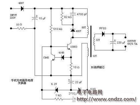
Power converter for mobile phone charger
Since the same name end of the winding is not indicated in the figure, it cannot be seen whether it is a forward or a flyback. However, from the structure of this circuit, it can be speculated that this power supply should be flyback. The 510KΩ at the left end is the starting resistor, which provides the base current for starting the switch.
The 10Ω resistor below 13003 is the current sampling resistor. The current is sampled and becomes a voltage (the value is 10*I). This voltage is applied to the base of transistor C945 via diode 4148. When the sampling voltage is greater than 1.4V, that is, when the switching tube current is greater than 0.14A, the transistor C945 is turned on, thereby lowering the base voltage of the switching tube 13003, thereby reducing the collector current, thus limiting the current of the switch and preventing The current is too large to burn out (in fact, this is a constant current structure, the maximum current of the switching tube is limited to about 140mA). The induced voltage of the winding (sampling winding) at the lower left of the transformer is rectified by a rectifying diode 4148, and the 22uF capacitor is filtered to form a sampling voltage.
For the convenience of analysis, we take the end of the emitter of the transistor C945 to ground. Then the sampling voltage is negative (about -4V), and the higher the output voltage, the more negative the sampling voltage. After the sampling voltage passes through the 6.2V Zener diode, it is applied to the base of the switching transistor 13003. As mentioned earlier, when the output voltage is higher, the sampling voltage is more negative. When it is negative to a certain extent, the 6.2V Zener diode is broken down, which lowers the base potential of the switch 13003, which will result in the switch tube. Disconnect or delay the conduction of the switch, thereby controlling the energy input into the transformer, thus controlling the rise of the output voltage and realizing the function of the regulated output. The lower 1KΩ resistor and the 2700pF capacitor in series are positive feedback branches. The induced voltage is taken from the sampling winding and applied to the base of the switching transistor to maintain oscillation.
There is not much to say about the secondary winding on the right. It is rectified by diode RF93 and filtered by 220uF capacitor to output 6V. The diode RF93 data was not found. It is estimated to be a fast return tube, such as a Schottky diode. Because the switching power supply has a higher operating frequency, a diode with an operating frequency is required. Here, a common Schottky diode such as 1N5816 or 1N5817 can be used instead. Also because of the high frequency, the transformer must also use a high-frequency switching transformer. The core is generally a high-frequency ferrite core with a high resistivity to reduce eddy currents.