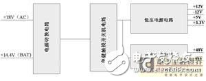
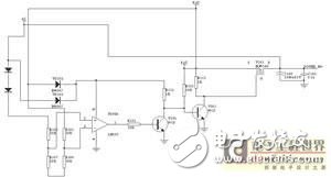
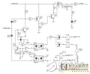
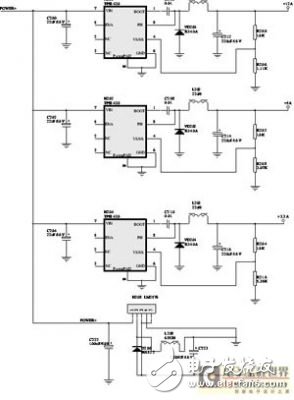
The power supply used inside the portable B-mode system is complex, and the power supply of the external adapter and battery must be DC/DC converted to convert to the voltage required by the system. In order to reduce the useless consumption on the power supply and improve the battery use efficiency, the power supply of the system main board, the B-mode control board, the liquid crystal display, and the keyboard is powered by a switching power supply. Figure 1 is a block diagram showing the overall design of a portable B-mode power supply. There are two kinds of portable B-power input voltage: one is the power adapter input, the voltage is 18V, the second is the battery input, the voltage is 14.4V. It is required to realize the hot switching between the two voltages, and does not affect the system operation when switching the voltage, that is, providing external power and battery power without delay hot switching function. Need to output ±12V, 5V, 3.3V, ±48V and other voltages, the specific indicators are 12V/2.5A, -12V/0.5A, 5V/4A, 3.3V/3A, +48V/80mA, -48V/80mA. With single button switch function, that is, when there is no power, press the power button to turn on the power; when there is power, press the power button to send a shutdown signal to the control panel, the host computer can also be shut down by software (that is, support ATX shutdown command). The power output interface uses a standard computer ATX interface. Figure 1 Block diagram of the overall design of the portable B-power supply Portable B-power switching circuit shown in Figure 2, in the external power adapter, the voltage input AC 18V, after the VD100, VD101 diode, and then divided by R100, R107 to the N100A (LM193) voltage comparator 3 feet ( In phase). The battery input voltage is 14.4V, which is divided by R101 and R108 and applied to the N100A (LM193) voltage comparator 2 pin (inverting terminal). Since the voltage of the 3 pin is higher than the 2 pin, the N100A (LM193) 1 pin outputs a high level, so that the transistor V100 is turned on, the V101 is turned off, the FET V105 is turned off, and the POWER_IN+ terminal obtains the 18V voltage of the external power adapter. When there is no external power adapter, or the portable B supercomputer is in use, the external AC power suddenly loses power and the external power adapter cannot be used. The N100A (LM193) pin 3 voltage is lower than 2 pins, and the N100A (LM193) 1 pin output is low. The level is such that the transistor V100 is turned off, V101 is turned on, and the field effect transistor V105 is turned on. The battery voltage is passed through the source and drain of the FET V105, and the POWER_IN+ terminal is the 14.4V voltage of the battery, which enables thermal switching between the two voltages. The VD102 and VD103 are isolated in the circuit to isolate the external power adapter and battery. Figure 2 power switching circuit The portable B-single-key touch switch circuit is shown in Figure 3. The POWER_IN+ voltage from the external adapter or battery is sent to the FET Q100 all the way to prepare for power-on, and the other is sent to the touch button POWER-KEY2 via R104 and VD104. One end. The other end of the POWER-KEY2 button is grounded. When the touch button POWER-KEY2 is pressed, the base of the transistor N106 is clamped at a low level, N106 is turned on, and N102 is also turned on, and the field effect transistor is turned on. Q100 is turned on, and the POWER_IN+ voltage from the external adapter or battery passes through the source and drain of the turned-on Q100 to obtain the POWER+ voltage, which supplies power to the high and low voltage circuits, and the machine is turned on. At the same time of power-on, the POWER+ voltage passes through a 6V Zener diode to turn on the transistor N104, and the N104 collector is at a low level, maintaining N106 conduction and maintaining the power-on state. Figure 3 single-button touch switch circuit When the portable B-mode is in the power-on state, when the button POWER-KEY2 is pressed again, the optocoupler B101 is turned on, the optocoupler is turned on, and the 4-pin of the inverter D101 outputs a low level to the control panel, and the control panel A low-level shutdown command POWER-OFF1 is issued to turn on the optocoupler B100, and the transistor N103 is turned on. The N104 is turned off, and the high level of the N104 collector turns off the N106, causing the FET Q100 to be turned off, and the shutdown is realized. When the host computer issues a high-level shutdown command POWER-OFF, the optocoupler B100 will also be turned on, and the rest of the process is the same as the control panel shutdown process. The portable B-mode low-voltage power supply circuit is shown in Figure 4. It consists of six TI's TPS5430 and one National Semiconductor's LM2576. The six TPS5430s provide two sets of +12V, +5V, and +3.3V voltages, one of which powers the main control board of the portable B-mode machine and the other set to power the computer in the portable B-mode. The two groups are exactly the same, so we only give a power supply schematic for one of the groups. The LM2576 is responsible for generating -12V to the computer in the portable B-mode. Figure 4 low voltage power supply circuit The TPS5430 has a wide voltage input range of 5.5 to 36V, a continuous 3A current output capability (peak up to 4A), and a conversion efficiency of 95%. The 8-pin small chip package has a metal heat sink on the back of the chip. It must be soldered to the ground when used. When the PCB is packaged, the heat sink is used as the 9th pin. There is no need to connect the heat sink, and the heat dissipation of the circuit board itself can achieve good results, which is especially suitable for the design and use of portable products. The 1 pin of the TPS5430 is the BOOT terminal and requires a low ESR capacitor of 0.01μF indirect at BOOT and 8 pin PH. 2, 3 feet are empty, 4 feet VSENSE is the feedback voltage terminal of the regulator, connected to the voltage dividing resistor end of the output voltage to obtain feedback of the output voltage. The 5-pin ENA is the power ON/OFF control terminal. When the voltage of this pin is lower than 0.5V, the chip will turn off the power conversion, and the supply current is reduced to 18μA. When it is suspended, the chip is working normally. We don't have this pin. Control, so the dangling is not connected. 6 feet grounded, 7 feet VIN is the power supply end, connected to POWER+. A high quality, low ESR ceramic capacitor indirectly in the power supply and ground. The 8-pin PH is the source of the internal power FET and is externally connected to the freewheeling diode and inductor. The 9th pin PowerPad is the heat sink metal on the back of the chip and must be connected to ground (GND). The output voltage of the TPS5430 is determined by the voltage divider of its 4-pin. The output voltage Vout = (1.221 + (R1 & TImes; 1.221) / R2) V. Among them, R1 is the voltage divider resistor and R2 is the voltage divider resistor. For the design of the TPS5430, R1 can take 10kΩ, and R2 can be calculated according to the output voltage to be obtained. According to R206 (1.11K), R208 (3.07K), R210 (5.36K) given in Figure 4, we can calculate the output voltage is 12.2V, 5.2V, 3.5V, respectively, slightly higher than the design value of 0.2V, load It is heavy and the voltage is just right when it is loaded. N208 (LM2576-12) is a product of National Semiconductor, 1 pin is the power supply terminal, connected to POWER+; 2 pin is the output terminal, external freewheeling diode and inductor; 3 pin is the ground terminal, 5 pin is the power ON/OFF control At the end, because the negative voltage is to be output, the 3rd and 5th pins are not grounded but connected to the -12V power supply; the 4th pin is the voltage feedback terminal, we use the fixed 12V output LM2576-12, so the 4 feet are grounded, no feedback is needed. Resistance divided. The portable B ultra-high voltage power supply circuit is shown in Fig. 5, and a DC/DC converter is used. The UA3843 is a high performance, fixed frequency, current mode controller specifically for DC/DC converter applications, providing designers with a cost effective solution with minimal external components. It is divided into PWM control, cycle current limit, voltage control and other parts. Figure 5 ±48V power supply circuit POWER+ supplies voltage to pin 7 of N1 (UA3843) via resistor R34, and the sawtooth oscillator formed by internal circuit R36, C33 and internal circuit of N1 starts working. The PWM pulse is output from pin 6 of N1, which controls the on-time of MOSFET V9 and determines the level of the output voltage. R37 is used to suppress parasitic oscillations, usually in series near the gate of the MOSFET. The gate resistor R37 cannot be too large, which directly affects the charge and discharge of the MOSFET input capacitor by the PWM drive signal, that is, affects the switching speed of the MOSFET. The induced electromotive force output from the secondary 9th and 10th pins of the switching transformer is rectified by VD14, and C35, L7, and C36 are filtered to form a +48V DC output voltage to supply power to the B-ultrasound probe. The induced electromotive force output from the 7th and 6th pins of the switching transformer is filtered by VD13, C39, L8, C37 to form a -48V DC output voltage for the B-ultrasound. VD12, C34, and R38 form a spike absorbing circuit for suppressing the extremely high amplitude spike caused by the drain of V9 at the moment when the switch is turned from on to off. The principle is: at the instant of V9 cutoff, the spike generated by the drain forms a charging loop through VD12 and C34, and the charging current suppresses the spike in a certain range, thereby avoiding the breakdown of V9 by the spike. When C34 is charged, C34 is discharged through R38, preparing for the next cycle to absorb the spike again. The 2-pin FEED BACK is the feedback voltage input. This pin is compared with the reference voltage of the non-inverting input of the internal error amplifier (generally +2.5V) to generate the control voltage. The width of the control pulse is grounded by this circuit. The internal error amplifier is used. The output pin 1 is controlled. The 3-cycle cycle current limit signal determines the width of the PWM pulse, which determines the level of the output voltage. N1 (UA3843) external pin R47, R48, R14, C32 constitute a cycle current limiting circuit, in each oscillation cycle, when the peak value of the 3 to 5 winding inductor current of the switching power supply pulse transformer L6 reaches the set value PWM pulse, the set value is determined by the voltage of the 1-pin COMP terminal of N1 (UA3843) (1 pin COMP is the output of the internal error amplifier). Usually a feedback network is connected between this pin and pin 2 to determine the gain of the error amplifier and Frequency response. The cycle current limit control process is as follows: the switch tube is turned on, the inductor current rises, and the sampling voltage V3 rises. When the voltage at pin 3 is greater than 1V, the internal current sense comparator flips, the internal PWM latch resets, the PWM pulse is turned off, and the PWM pulse is ready to enter. cycle. In order to eliminate the spike of the current limiting circuit, a sharp wave filter circuit is formed by R14 and C32 to ensure that the cycle current limiting function is effective in every oscillation period. R47 and R48 are current-limiting sampling resistors, which determine the maximum output current value of the entire switching converter. Changing the resistance value can adjust the maximum output current. N1 (UA3843) is a current-mode pulse width modulator with two closed loop controls. The current sampling signal is sent to the non-inverting input terminal of the current detecting comparator to form a current closed-loop control. The error voltage is sent to the output pin 1 of the internal error amplifier, and the output is sent to the inverting input terminal of the current detecting comparator as a comparison reference. Voltage closed loop control. It can be seen that the voltage closed loop and the current closed loop interact, and both of them finally control the PWM latch through the current sense comparator, that is, control the width of the PWM pulse. The voltage closed-loop control circuit is composed of voltage reference N2 (TL431A), photocoupler B4 (TLP521), and resistors R31, VR7, R12, R32 and other components. The current signal output from the photocoupler B4 (TLP521) is converted into a voltage signal and sent to the output pin 1 of the internal error amplifier. The internal comparison of the N2 (TL431A) error amplifier is 2.5V. The voltage closed-loop voltage regulation control process is: the output voltage rises, the TL431A reference terminal VR rises, the TL431 turns on, the photocoupler B4 (TLP521) turns on, the 1 pin voltage drops, the internal current detection comparator flips ahead, and the internal PWM lock The memory is reset in advance, the PWM pulse is narrowed, and the output voltage is lowered, thereby stabilizing the output voltage. The high voltage output voltage value VOUT=(1+R31/(R12+VR7))Vref. By adjusting the value of the potentiometer VR7, the output can be adjusted to ±48V, and the adjustment range is 31&TImes; 2.5=77.5V~(1+15) &TImes;2.5=32V. This paper introduces the design of portable B-mode power supply, including the design of power switching circuit, the design of single-button touch switch circuit, the design of low-voltage power supply circuit and the design of high-voltage power supply circuit. The design specifications are well completed in our portable devices and can be applied to other portable devices. The plug of the aerospace Cable Assembly is divided into male and female. The specific identification method is as follows:
How to wire the aerospace cable assembly plug?
Radiation-resistant film-wrapped insulated wire for aerospace: suitable for aerospace vehicles. The wire is irradiable and can be used in an environment where radiation such as current market rays exists.
We cooperate with all leading cable and connector manufacturers, and have a wide range of professional equipment, allowing us to provide quality wiring harness and cable assembly, quick delivery time and favorable prices!
In addition to Aerospace Cable Assembly, we also have Vehicle cable assembly and Industrial Cable Assembly.
Welcome companies from all over the world to contact us. We will serve you with the greatest enthusiasm and become your Chinese partner.
Aerospace Cable Assembly,Military Aerospace Cable Assembly,Aerospace Military Wire Harness,Aerospace Wire Harnesses Kable-X Technology (Suzhou) Co., Ltd , https://www.kable-x-tech.com


1. One side of the plug (the protruding Connector) is a male head, and one side of the jack (the concave connector) is a female head.
2. Distinguish from the appearance and shape, the pointed part of the head is generally a male terminal, and the head with a round hole is generally a female terminal.
3. It can be distinguished by size: generally the larger head is the female head, and the smaller head is the male head.
1. In general, there will be a semi-circular splint at the back of the conventional aviation plug to fix the lead, and there will also be two small turnbuckles on it. You can use a tool to remove the nut and then separate the deck.
2. After removing the aviation plug splint, find a thin nail as a tool and put it into the jack to fix it, and rotate the aviation plug in the opposite direction on one side, so that the core and wire of the aviation plug can be naturally pulled out from the front.
What are the test contents for aerospace cable assembly?
When conducting aviation wiring harness testing, we mainly conduct the following wiring harness tests:
1. On-off test
2. Withstand voltage test
3. Insulation resistance test
4. Two-wire/four-wire resistance test
5. Instantaneous interruption test
Tinned copper core PFEP insulated wire and cable: It is mainly used in aircrafts, aircrafts or installation wires used in harsh environments such as high temperature and strong corrosion. It has good high temperature and corrosion resistance characteristics.
Aeronautical radiation-resistant low-temperature flexible wire: It is wrapped with special composite film for insulation, woven with synthetic fibers, and treated with special paint. The wire can still maintain good flexibility and electrical insulation performance after being tested at -196 ℃ dynamic bending, high and low temperature impact, and irradiation.
