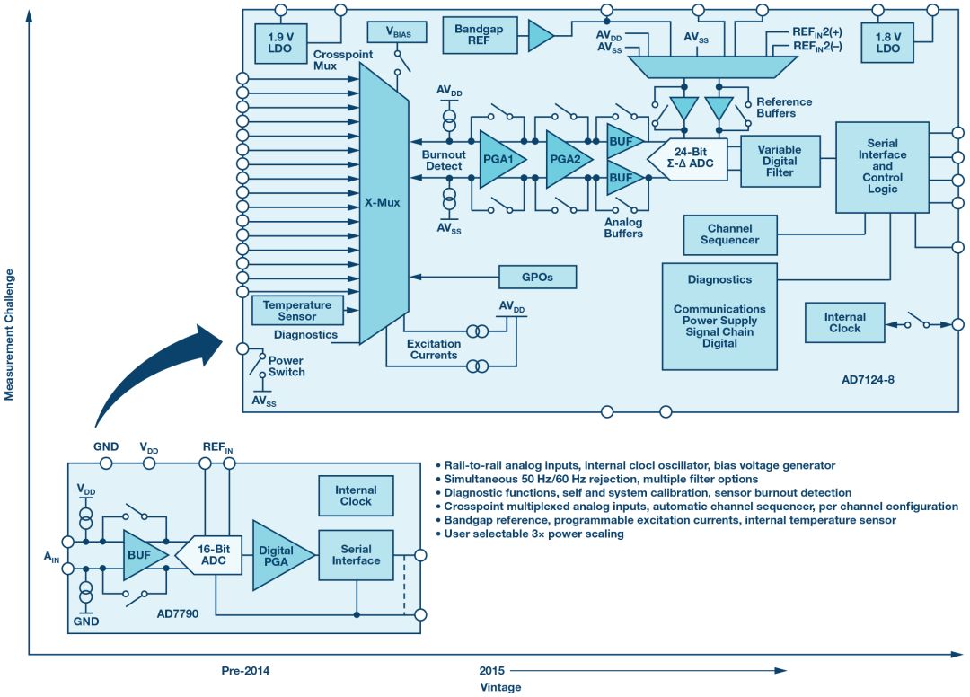
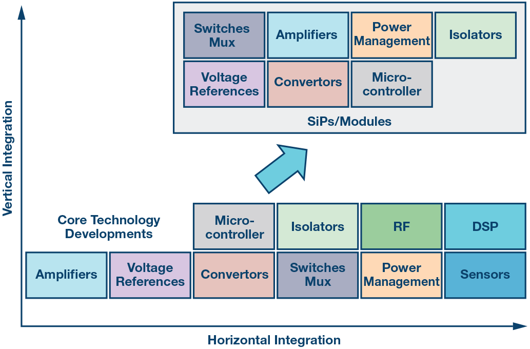
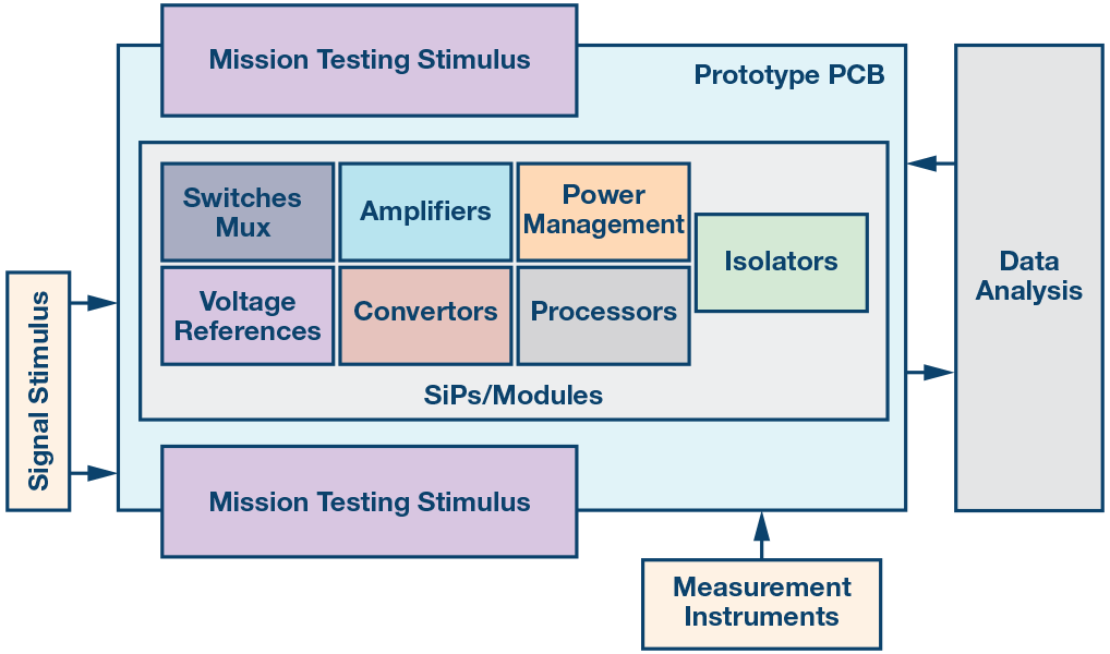
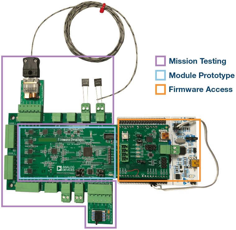
Have you ever wondered what the accuracy of a measurement chip means for a test bench measurement engineer? When we are still a student, the principle of observance is that the accuracy of the measurement system needs to be at least 10 times higher than the device itself. This is still a challenge today. How can we improve the level through test stations that we may never have considered? Members of the ADI Engineering Survey team here provide you with some relevant professional insights. Over the years, "to go one step further" has been implicit in ADI's corporate strategy. Today, this strategy is increasingly clear. We used to provide only discrete devices and data sheets. Today our new concept is to participate in and understand all the problems we have to solve for our customers. As part of the new concept, ADI's measurement engineering has gone beyond the traditional method of testing only ICs to test solutions, including software, signal chain systems in packages, micro-modules, and other components. This approach will ensure that the solutions we develop will create significant value for our customers. Within ADI, measurement engineering teams are sometimes seen as the people who develop hardware and software to launch products. However, the measurement department consisting of test and evaluation engineering is one of ADI's most challenging engineering specialties. Measurement engineers are the basic personnel supporting the relationship between the company and its customers. They are the people you trust when looking at guaranteed maximum and minimum device specifications, typical performance, maximum ratings, and robustness. As design performance continues to improve, we rely on the experience of measurement engineers to keep pace with improvements in all aspects of performance (speed, noise, power consumption, or new integration features). The measurement profession consists of testing and evaluation projects. The challenges faced include breakthrough performance, on-time delivery, and ever-increasing quality requirements. Not so long ago, we were dealing with a simple single-function IC (converter) with 10 or 12 bits of precision. Today, 20-bit SAR converters, 20-bit DAC converters, and 32-bit sigma-delta converters show how measurement challenges have changed over the past few years as IC technology has evolved. To clarify the degree of change, we will examine the evolution of low-power sigma-delta products to help illustrate the integrity of the signal chain integration achieved, and highlight the requirements and advancements that this brings to our measurement capabilities. We now hope to bring SiP (systematic packaging), micro modules and modules to the next level, and customers will once again present us with new measurement challenges that will force us to improve measurement methods and develop novel test and measurement solutions. SiP uses complex core technologies to integrate passive and active devices (sometimes also integrating a central processing unit to perform configuration and control) to achieve an unprecedented level of system integration. This level of integration introduces more and more features, embedded feature combinations, advanced packaging, internal node access issues, embedded software, system-level calibration, and more. These solutions simplify the use of complex converter products, and their complexity and design and measurement barriers are handled and resolved within ADI. Past, now A typical example of the latest test and measurement challenges is the progress of our low-power sigma-delta family. In order to demonstrate the progress made, Figure 1 highlights the fact that our systemic chip level is now much higher than previous generations of converters. The latest product in this product family is a low-power, low-noise, fully-integrated analog front end for high-precision measurement applications. The product's signal chain integration requires 24-bit sigma-delta ADC field, reference performance and accuracy, channel serialization and timing, digital features and functional aspects, and oscillator performance measurement experience. For comparison, Figure 1 also shows a previous typical 16-bit device that was considered to have breakthrough performance at the time. The related challenges have been solved and today's technology has been improved by several orders of magnitude. Unless technological advances match our testing and measurement capabilities, we will not be able to maintain industry technology leadership. Figure 1. Evolution of integration; performance improvement drives innovation An in-depth understanding of the converter architecture, expertise in mixed signal test circuit design, PCB layout techniques, and measurement software allows us to get the best performance from these highly integrated converters. This facilitates the development of SiP/modules, allowing our experience to be used to solve more customer design challenges and shorten development time. Now, the future As we move forward and tackle the future of our customers, our toolbox is full of rich product and measurement expertise. Throughout ADI's history, we have continued to make breakthroughs in actual signal processing and continue to expand our core technologies through on-chip integration. In recent years, we have begun to enter the field of DSP, RF and MEMS, and opened up new horizons in emerging areas such as the Internet of Things. ADI's acquisition of Linear Technology is a further step, integrating our strong product portfolio and adding industry-leading high-performance analog and power solutions. This reinforces our position to integrate these technologies and influence customers through solutions that truly demonstrate our capabilities. Figure 2 shows our progress in accumulating technology horizontally and vertically. We are now using these building blocks in SiP/module development to provide solutions beyond silicon. Measurement engineers support this goal by integrating our expertise in these core technologies. Figure 2. SiP/module development leverages our core technology Why does ADI think this is necessary? From our contacts with customers, we know that they are also developing, and customers are even higher. The layout is changing, your mixed-signal design team may be smaller, you may have other concerns and expertise, and you are looking for ways to shorten the design cycle and time to market. By providing a complete signal chain, ADI can help you get rid of these design challenges, which require effective measurement solutions as a support. Module Solution Prototyping By working with customers as early as possible, measurement engineers can use our hardware expertise to prototype SiP/module development. We can proof-of-concept the novel ideas and quickly debug and evaluate, if necessary, iterating the schematics and layout for optimal performance. We can perform mission tests, evaluate customer's sensors, test the entire system in specific application scenarios, and analyze the data to ensure that all requirements are met before developing the final SiP or module. Figure 3. Module test prototype With these prototypes, we can also develop ATE solutions to overcome new test challenges that system-level devices may pose, such as package size, test node access points, or firmware interfaces. With our experience with the core technology of the modules that make up these products, we can use these device grades to achieve the best performance for these devices and even bring system-level performance to a new level. Through prototypes, we can easily interface with reference excitation signals and measurement instruments and evaluate which test nodes need to be accessed for production testing. This prototype allows us and our customers to start verifying the system-level calibration of the entire system signal path. Figure 4. Example of a prototype board for module testing With the development of SiP/modules, processors are required to complete configuration, control, and algorithm processing. In order to simplify the complexity and eliminate the burden on customers, firmware may need to be developed. This can start and evolve with the prototype. By developing and testing firmware, measurement engineers use their troubleshooting thinking patterns to detect errors and predict situations that may cause problems. This can be fed back into system design and progress. This prototype can be used to present ideas to customers, stimulate feedback, and then determine the direction of the module. In this way, customers can influence the solution from an early stage. Conclusion Over the years, as the complexity and integration of core technologies continues to grow, the capabilities of the ADI measurement team have also increased. We are testing more than just core converters. The increase in chip integration has in turn promoted the progress of measurement techniques and techniques. Our measurement solutions in laboratories and production tests have advanced as technology has advanced. Combining our measurement expertise in core converters, sensors, amplifiers, voltage references, power supplies and digital circuits, we are able to surpass all possibilities. Looking ahead, with the continuous development of multi-chip SiPs, modules and micro-modules, ADI will continue to climb the peak. These modules allow the technology to take a higher level, bringing new challenges to measurement engineering, but also reducing the engineering burden on our customers. Simplifying customer application development is a central task of ADI technology. We have expanded and will continue to expand our measurement technology to take full advantage of our expertise to support these new technologies. Whether through prototype PCB design, task testing, firmware development, or prototype demonstrations, ADI's measurement engineers are the key to the success of these products. As our technology products progress faster, the ADI measurement team will take a step forward and ensure that world-class measurements are accompanied by world-leading technologies.
If you are tired of the original back of your phone, you should try our 3D Relief Back Sticker. The Back Skin Protective Film on the back can not only bring you a visual change, but also protect the back cover of the phone itself from scratches and collisions. Real 3D touch, personalized and stylish pattern design. Bring you a perfect experience.
In daily use, it can protect the equipment from scratches, dust, impact and other damage.
Long-lasting anti-scratch effect, significantly reducing dust, oil stains and fingerprint stains.
Easy to install, easy to stick to the back of the phone, and will not damage the original appearance of the phone.
With the Protective Film Cutting Machine, you can install the Back Film on different types of mobile phone back shells, including mobile phones, tablet computers and other electronic products. Customization can be completed in 30 seconds with just one click.
If you want to know more about 3D Relief Back Sticker, please click product details to view the parameters, models, pictures, prices and other information about 3D Relief Back Sticker.
Whether you are a group or an individual, we will try our best to provide you with accurate and comprehensive information about 3D Relief Back Sticker!
3D Phone Sticker, Carbon Fiber Back Sticker, 3D Relief Back Sticker, 3D Printing Back Sticker, Phone Skin,Mobile Phone Back Sticker Shenzhen Jianjiantong Technology Co., Ltd. , https://www.jjthydrogelprotector.com


