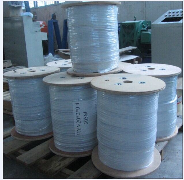
Description Technical data Standards and performances  Packing &delivery 1) Length:305m/roll, other length is available according to clients request. 2) Packing: wooden drum 3) Other packing available according to client's request Delivery Detail: 7-15 days after receiving 30% T/T or L/C Company Introduction Area 8000 m² Number:100 ( Including 10 technical personnel) Our company was established in 2002 and is a professional manufacturer of Lan cable, patch cord cable, fiber optic cables, coaxial cables, alarm cable, telephone cables, power cables, fiber patch cord s, connectors and accessories. Main Markets We also attend the canton fair twice one year.  Description Technical data Standards and performances  Packing &delivery 1) Length:305m/roll, other length is available according to clients request. 2) Packing: wooden drum 3) Other packing available according to client's request Delivery Detail: 7-15 days after receiving 30% T/T or L/C Company Introduction Area 8000 m² Number:100 ( Including 10 technical personnel) Our company was established in 2002 and is a professional manufacturer of Lan cable, patch cord cable, fiber optic cables, coaxial cables, alarm cable, telephone cables, power cables, fiber patch cord s, connectors and accessories. Main Markets We also attend the canton fair twice one year.  HDI PCB Specification
High density interconnect (HDI) PCBs represent one of the fastest-growing segments of the printed circuit board market. Because of its higher circuitry density, the HDI PCB design is able to incorporate finer lines and spaces, smaller vias and capture pads, and higher connection pad densities. A high density PCB features blind and buried vias and often contains microvias that are .006 in diameter or even less.
The HDI PCBs we offer include the following highly requested characteristics:
Applications
HDI PCB is used to reduce size and weight, as well as to enhance electrical performance of the device. HDI PCB is the best alternative to high layer-count and expensive standard laminate or sequentially laminated boards. HDI incorporate blind and buried vias that help to save PCB real estate by allowing features and lines to be designed above or below them without making a connection. Many of today's fine pitch BGA and flip-chip component footprints do not allow for running traces between the BGA pads. Blind and buried vias will only connect layers requiring connections in that area.
HDI PCB HDI PCB,Special HDI PCB,HDI Prototype PCB,HDI Board PCB Storm Circuit Technology Ltd , http://www.stormpcb.comÂ
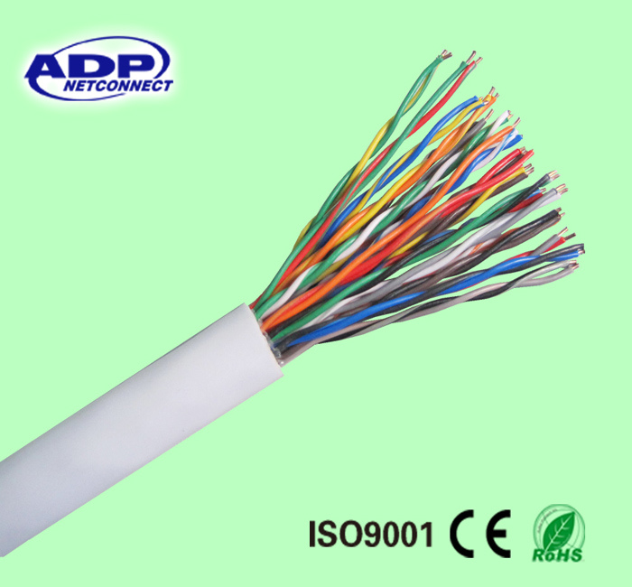
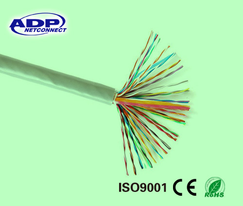
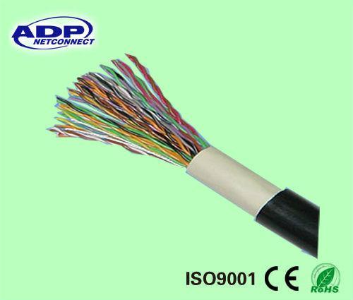
Â
Our total manufacturing area is 8000 square meters, with a lot of equipment, such as high speed cross product lines, high speed cross supervisor data return line systems and a cat6 twister system.Â
Our products strictly adhere to ISO9001, CE and ROHS international standards, also covering our design, development, service and management. We have more than 100 employees, including 10 technical personnel. Our annual production value reaches USD 2000,000,000, giving us stable development and increased competitive power within the markets.Â
ADP enterprise has been and will always be committed to the development and promotion of independent brands.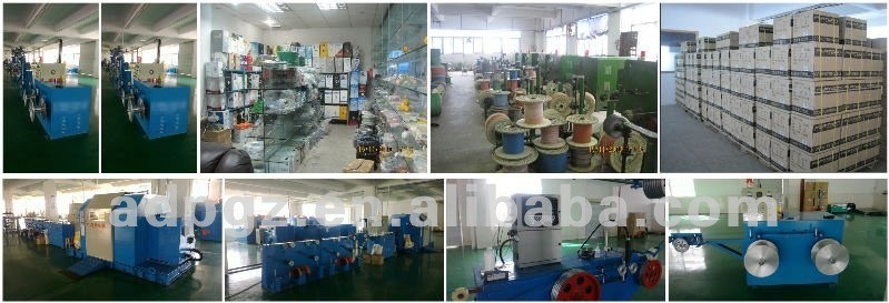
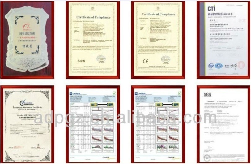
Our products strictly adhere to ISO9001, CE and ROHS international standards,Certificate: UL/CE/ROHS/SGS/ISO9001
Â
South America, Russia, Mid East, Eastern Europe, AfricaÂ


Â
Our total manufacturing area is 8000 square meters, with a lot of equipment, such as high speed cross product lines, high speed cross supervisor data return line systems and a cat6 twister system.Â
Our products strictly adhere to ISO9001, CE and ROHS international standards, also covering our design, development, service and management. We have more than 100 employees, including 10 technical personnel. Our annual production value reaches USD 2000,000,000, giving us stable development and increased competitive power within the markets.Â
ADP enterprise has been and will always be committed to the development and promotion of independent brands.

Our products strictly adhere to ISO9001, CE and ROHS international standards,Certificate: UL/CE/ROHS/SGS/ISO9001
Â
South America, Russia, Mid East, Eastern Europe, Africa
HDI PCBs are characterized by high-density attributes including laser microvias, fine lines and high performance thin materials. This increased density enables more functions per unit area. Higher technology HDI PCBs have multiple layers of copper filled stacked microvias (Advanced HDI PCBs) which creates a structure that enables even more complex interconnections. These very complex structures provide the necessary routing solutions for today's large pin-count chips utilized in mobile devices and other high technology products.
Blind and/or buried vias
Via-in-pad
Through vias from surface to surface
20 µm circuit geometries
30 µm dielectric layers
50 µm laser vias
125 µm bump pitch processing
Model NO.: Cat3 Telelphone Cable
Wire Core Material: Bare Copper Wire
Certification: CE, ISO, RoHS, CCC
Model: HYA
Brand: ADP/OEM
Transport Package: Wooden Reel
Specification: 0.5mm
Origin: Guangdong
HS Code: 8517699000
Model NO.: Cat3 Telelphone Cable
Wire Core Material: Bare Copper Wire
Certification: CE, ISO, RoHS, CCC
Model: HYA
Brand: ADP/OEM
Transport Package: Wooden Reel
Specification: 0.5mm
Origin: Guangdong
HS Code: 8517699000
Cable photos
ADP cable manufacturer
Certificate
Good Service
Over 14 years of factory experience
Over 6 years of foreign trade experience
Direct factory price
Professional one -to-one service
Perfect customer service
OEM is available
Various products range
Â
 Any inquiry, just feel free to contact with us any time!