Class D audio amplifier has the advantages of high efficiency, energy saving and miniaturization, and is widely used in many fields such as portable products, home AV equipment and car audio. The class-D audio power amplifier designed in this paper is mainly based on the following three considerations: ensuring high fidelity, improving efficiency and reducing size. This article designs a class D audio power amplifier that works at 5V power supply voltage and uses PWM to implement. The whole system includes input amplifier stage, error amplifier, comparator, internal oscillation circuit, drive circuit, full-bridge switching circuit and reference circuit. . By introducing feedback technology to reduce the THD index of the system, the dual inverse wide modulation scheme not only suppresses the static power consumption of the class D audio power amplifier, but also achieves the purpose of removing the low-pass filter at the output end of the class D audio power amplifier. Reduced the size of the system. The system structure of the class-D audio power amplifier designed in this paper is shown in Figure 1. The amplifier structure is based on the bilateral natural sampling technology solution. At any time, the output contains twice the amount of information as the unilateral sampling scheme. Through bilateral natural sampling, a large amount of distortion components in the output audio signal can be removed to Outside the audio bandwidth range that can be sensed by the human ear, the purpose of removing the low-pass filter at the output end of the class D audio power amplifier is achieved. The system uses a single power supply. The high and low levels of the pulse signals "out1" and "out2" are VDD and GND, respectively. The input amplifier stage is realized by the closed-loop structure of the operational amplifier OTA, and the error amplifier is composed of the operational amplifier OTA and the capacitor Cs. When the system is working, the audio input signal Vin first passes through the input amplifier stage and then outputs two differential signals, then sums with the feedback signal and sends to the error amplifier to generate error signals VE1 and VE2, modulate the triangular wave carrier signal VT and output two pulses The signals "out1" and "out2" drive the speaker to sound. The system contains two feedback loops, the first one is composed of R1, Rf1 and OTA, used to set the input amplifier stage and the gain of the entire class D audio power amplifier, the second one is composed of R2, Rf2 and the back-end audio signal processing circuit , Used to reduce the THD index of the system. In Figure 1, the currents I1 and I2 that charge and discharge the capacitor Cs are determined by Vout1, Vout2, Vin, R1, Rf1, R2 and Rf2. The resistance and capacitance must have good linearity and matching to obtain a good Closed-loop performance. The model of the open-loop class D audio power amplifier is shown in Figure 2. The system output is: The total harmonic distortion of the open-loop system is: In equation (2), Vin is the input signal of the amplifier, Vn is the introduced harmonic distortion, and Hf is the transfer function. The model of Class D audio power amplifier with feedback loop is shown in Figure 3. The output of the system at this time is: Hfb is the transfer function of the closed-loop model, and G is the feedback gain. In order to obtain equal magnification, the design transfer function is: Then formula (3) becomes: The total harmonic distortion of the closed system is: Comparing equation (2) and equation (6), it can be seen that the closed-loop system THD with feedback loop is 1 / (1 + HfbG) of the open-loop system THD, that is, the THD of the system is reduced by the feedback structure. The system unit circuit mainly includes: input amplification stage, error amplifier, comparator, drive circuit, full-bridge switching circuit, internal oscillation circuit and reference circuit. The input amplification stage of the class D audio power amplifier is implemented based on the closed-loop structure of the operational amplifier (OTA). Its structure is shown in Figure 4. It is used to perform level adjustment and signal amplification processing on the input audio signal as required The input signal can meet the requirements of the subsequent circuit in terms of amplitude. The gain of the input amplifier stage can be determined by setting the resistance of Rf1 and R1. The comparator circuit used in this article is shown in Figure 5. The comparator circuit consists of three stages, namely the input pre-amplification stage, judgment stage (or positive feedback stage) and output digital shaping buffer stage. The pre-amplification stage is implemented by a differential amplifier with active load, and its amplification factor is not very large. It is used to amplify the input signal to improve the sensitivity of the comparator, and the input signal of the comparator and the switch from the positive feedback stage The noise is isolated; the judgment stage is used to further amplify the signal of the pre-amplification stage. It is the core part of the comparator. In the circuit, the positive feedback is realized by cross-connecting the gates of m8 and m9 to have the ability to distinguish very small signals. Ability and increase the gain of this stage circuit; the output buffer stage is a self-biased differential amplifier, its input is a pair of differential signals, used to convert the output signal of the judgment stage into a logic level (0V or 5V) Namely output high level VOH = VDD, output low level VOL = GND. Figure 5 Comparator circuit diagram The structure of the triangle wave generating circuit used in this paper is shown in Figure 6, where m5, m6, m7, and m8 constitute two sets of constant current sources, and m9 ~ m13 and Q1 constitute the output stage. In the circuit, the output signal VT is fed back to the comparators comp1 and comp2, respectively, and the reference levels VREF1 and VREF2 (VREF2 It can be seen from Figure 6 that the initial voltage value of VT is zero. The output stage is realized by a full-bridge switch circuit composed of N and P-type power switch pairs. Its structure and load current flow are shown in Figure 7. The full-bridge switching circuit works in the switching mode. With the change of the input signal, the state of m1 ~ m4 changes accordingly. Only one pair of diagonal power switch tubes is always on and the other pair is off. The drive circuit structure is shown in Figure 8. This circuit can effectively adjust the dead time (N-type and P-type power switch tubes are turned off at the same time), prevent single-arm "shoot-through" phenomenon, and have a protective shutdown function. The input signal is the PWM pulse signal output by the comparator. PWM1 is used to drive the N-type power switch, and PWM2 is used to drive the P-type power switch. In order to avoid the single-arm "shoot-through" phenomenon in the full-bridge switching circuit, when the PWM signal changes from low level to high level, PWM2 should first change to high level, turn off the PMOS power switch, and then PWM1 changes again When it is high level, turn on the NMOS power switch, as shown in Figure 9; conversely, when the PWM signal changes from high to low, PWM1 changes to low level first, turn off the NMOS switch power tube, and then PWM2 changes to low Level, turn on the PMOS switch power tube. In the actual circuit, the length of the dead time can be adjusted by controlling the control bit Tc of the delay unit as needed. In order to reduce distortion, the dead time must be reduced. The drive circuit uses a step-by-step increase in drive capacity to drive the power tube, thereby reducing the necessary dead time and ensuring low distortion. EN is the enable signal of the control module, which normally works at a high level; when over-current, over-temperature, etc. occur, it becomes a low level, turning off the full-bridge power switch circuit. The structure of the bandgap voltage reference source designed in this paper is shown in Figure 10, which is mainly composed of the core circuit and the startup circuit. In the core circuit, M1 ~ M12 together form a cascode current mirror to provide DC bias. The op amp op1 uses two-stage cascode amplification. In addition, the negative feedback is introduced in the circuit of FIG. 10, which ensures the accuracy of the current mirror of the bias circuit, and is independent of the power supply, and has a high power supply rejection ratio. When the circuit is powered on, there may be zero current in the bias circuit, and the circuit needs to be started to ensure that the circuit can work normally. When the circuit is not working, EN and Vs1 are 0, Vs2 and Vs3 are 1, M15 and M17 are not connected, the op amp output is high, and M3 ~ M6 are not connected, and the entire circuit does not consume current. When EN changes from 0 to 1, due to the effect of C1, Vs1 remains at 0, Vs2 is at 1, Vs3 becomes 0, at this time M15 and M17 are turned on, inp and inn are pulled to 0 and 1, respectively, and the op amp outputs When it becomes 0, M3 ~ M6 are turned on, M13 and M14 branches start to charge, and charge C1 until Vs1 is higher than the threshold voltage of I2, Vs2 becomes 0, Vs3 becomes 1, M15 and M17 are turned off. Eventually, the circuit deviates from the zero current state and starts to work normally, and Vs1 is charged to the power supply voltage, and the entire startup circuit no longer consumes current. This paper studies the working principle of class D audio power amplifier based on PWM modulation technology, reduces the THD of class D audio power amplifier by introducing feedback technology; reduces the necessary dead time by increasing the driving capacity step by step, and guarantees Lower distortion; adopting dual inverse wide modulation scheme, on the one hand, suppresses the static power consumption of the system, on the other hand, removes the LC low-pass filter of the output stage, and achieves the purpose of reducing system cost and volume. Twinkle System Technology Co Ltd , https://www.pickingbylight.com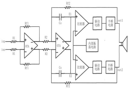
Figure 1 Class D audio power amplifier structure 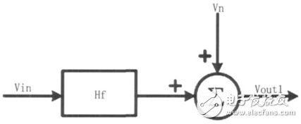
Figure 2 Open-loop class D audio power amplifier model 

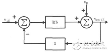
Figure 3 Closed-loop class D audio power amplifier model 


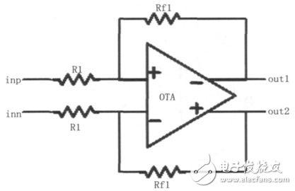
Figure 4 Input amplifier circuit structure 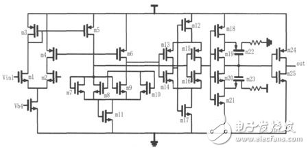
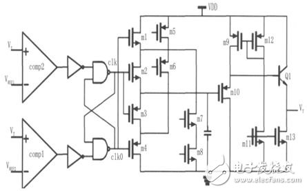
Figure 6 Triangle wave generating circuit 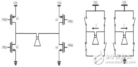
Figure 7 Schematic diagram of the full-bridge circuit structure and load current 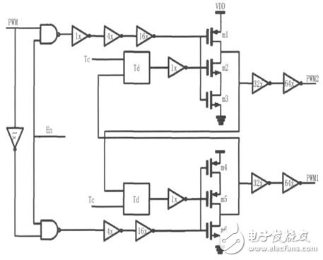
Figure 8 Drive circuit structure 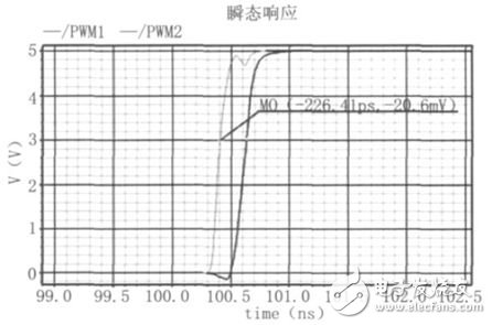
Figure 9 Dead time 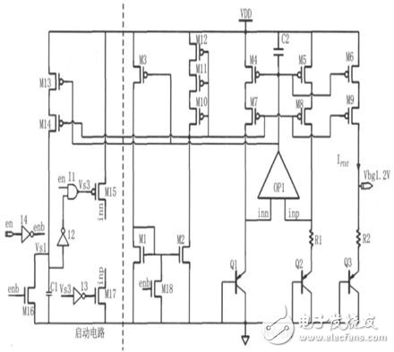
Figure 10 Reference circuit
Central Topic: System Design of Class D Audio Power Amplifier Circuit Design and Implementation of Class D Audio Power Amplifier Unit Solution: Circuit Design of Class D Audio Power Amplifier Unit