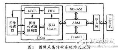
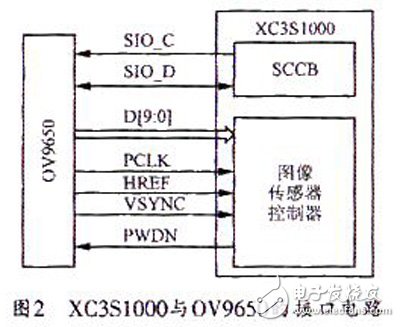
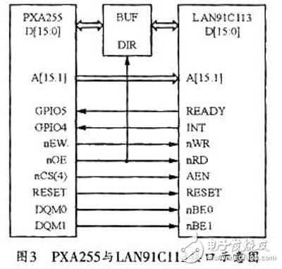
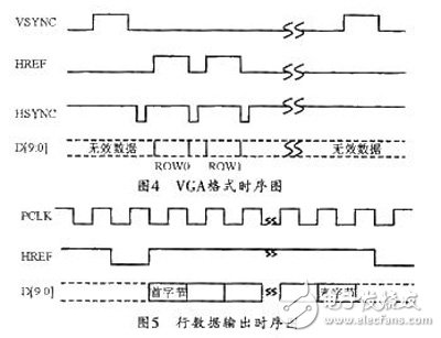
The rapid development of image processing technology has made image acquisition and processing systems more and more widely used in improving the automation level of agricultural production. The current image acquisition systems are based on CCD cameras, image acquisition cards and computers, some based on CCD cameras, decoders, FPGAs and DSPs, and some based on CMOS image sensor chips, FPGAs and DSPs, which are real-time and flexible. There are advantages and disadvantages in terms of maintainability. In agricultural production, systems based on CCD cameras, image acquisition cards, and computers are mostly used. This paper combines the front-end image processing and image data transmission needs in the actual system. Taking full advantage of the flexibility of ARM and the parallelism of FPGA, a fast image acquisition and transmission system based on ARM+FPGA is designed. The selected ARM (Ad-vanced RISC Machines) architecture is a 32-bit embedded RISC microprocessor architecture with a rich instruction set and flexible programming. FPGA (Field ProgrammableGate Array) has great advantages in speed and parallel computing, and is suitable for real-time requirements of image processing. This article uses Intel's Xcale PXA255 and Xilinx's Spartan-3XC3S1000 to implement the system design. The structural block diagram of this system is shown in Figure 1. In the figure, the image sensor module is responsible for image acquisition, the FPGA is used to control the CMOS image sensor chip, the ARM is responsible for image data exchange, the Ethernet chip control and the UDP/IP protocol implementation, and the Ethernet module mainly implements Ethernet data transmission, SDRAM. Used to store image data, FLASH is program memory. When the system works, the data collected by the CMOS sensor is first stored by the FPGA into the dual-port SRAM, and then the ARM reads the data from the dual-port SRAM of the FPGA and stores it in the SDRAM. After storing one frame of image data, the ARM passes through the Ethernet. The chip sends the data to the host computer. This system uses OV9650 as the image acquisition sensor. The OV9650 is Omni Vision's color CMOS image sensor that supports SXVGA, VGA, QVGA, QQVGA, CIF, QCIF, QQCIF mode and SCCB interface, and features automatic exposure control, automatic gain control, auto white balance, and automatic bandpass filtering. Automatic black level calibration and other functions. The maximum frame rate of the OV9650 is 30 fps in VGA format and 15 fps in SXVGA format. This system uses VGA format. FPGA is mainly used for image sensor control, image data buffering and peripheral chip timing generation. Taking into account the implementation of the image processing algorithm, the system selected Xilinx's XC3S1000, which belongs to the SPARTAN-3 series, with a capacity of 1 million gates. In this design, the FPGA typically runs at 80 MHz. The interface circuit diagram of XC3S1000 and OV9650 is shown in Figure 2. The internal structure of the FPGA includes a CMOS control unit, an SC-CB interface unit, a dual-port RAM unit, a FIFO unit, and the like. The CMOS control unit further includes a frame synchronization module, a field synchronization module, a pixel clock module, and the like. The ARM processor of this system uses PXA255 for functions such as image data exchange and Ethernet data transmission. The PXA255 is a microprocessor based on the fifth-generation ARM RISC architecture ARMV5TE from Intel. The CPU runs at up to 400 MHz, has a 32 KB instruction cache, a 32 KB data cache, a 2 KB micro Cache, and has a rich serial peripheral interface and supports a variety of memory chips. The system uses two SDRAMs and two FLASH memories, of which SDRAM is used for image data temporary storage. The system uses SAMSUNG K4S561632C-TC75 with a capacity of 32 MB. The FLASH program memory uses Intel's E28F128J3A-150 as the NOR FLASH with a capacity of 16 MB. The Ethernet chip of this system is LAN91C113. This is the Fast Ethernet 10/100 Mbps controller from SMSC, which supports a variety of embedded processor host interfaces. The LAN91C1B has an internal 8 KB FIFO that can be used to receive and transmit data. In addition, the LAN91C113 chip also integrates the MAC (Media Access Control Layer) and PHY (Physical Layer) of the CSMA/CD protocol, and the IEEE802.3/802.3u-100BASE-TX/10Base-T specification. In this system, the serial EEPROM interface of LAN91C113 is connected to AT93C46. The PXA255 access LAN91C113 adopts the asynchronous static memory mode, and the address enable signal AEN of the LAN91C113 is connected to the static chip chip selection of the PXA255. Figure 3 shows the interface between PXA255 and LAN91C113. The data output of the OV9650 uses the Bayer raw data output format, and each pixel outputs only one color at a time. The odd scan lines output RGRG..., the even scan lines output GBGB.... The FPGA is responsible for the acquisition of image sensor data. After power-on, the system first initializes the CMOS image acquisition chip to determine its mode of operation. These parameters are controlled by the corresponding register values ​​within the OV9650. The FPGA completes the parameter configuration by controlling the SCCB bus. After the system is configured, image data can be collected. Figures 4 and 5 are timing diagrams of data acquisition and output. Where VSYNC is the field sync signal. HREF is a horizontal sync signal. PCLK is a pixel data output sync signal. When HREF is high, effective data acquisition can be started, and the falling edge of PCLK indicates the generation of data. For every falling edge of PCLK, the system transmits one bit of data. The system can transmit a total of 640 bits of data while HREF is high. In one frame of image, that is, when VSYNC is low, HREF will appear 480 times high. The arrival of the rising edge of the next VSYNC signal indicates the end of the image acquisition process at resolution 640 & TImes; 480. DLP Home Projecror-The principle is mainly to switch the light through the control of the micro-mirror, so as to realize the color scale and gray scale. On the small DMD chip, there are nearly a million small mirrors that are smaller than the hair The advantages of DLP projectors are: long service life and fast response speed Dlp Home Projecror,dlp projector remote,dlp projector portable,dlp 1080p projector,dlp projector 4k Shenzhen Happybate Trading Co.,LTD , https://www.happybateprojector.com


