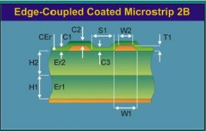
As PCB signal switching speeds continue, today's PCB designers need to understand and control the impedance of PCB traces. Corresponding to the shorter signal transmission times and higher clock rates of modern digital circuits, PCB traces are no longer simple connections, but transmission lines. In the actual case, it is necessary to control the trace impedance when the digital marginal speed is higher than 1 ns or the analog frequency exceeds 300 Mhz. One of the key parameters of a PCB trace is its characteristic impedance (ie, the ratio of voltage to current as the wave travels along the signal transmission line). The characteristic impedance of the conductor on the printed circuit board is an important indicator of the board design. Especially in the PCB design of the high-frequency circuit, it must be considered whether the characteristic impedance of the wire and the characteristic impedance required by the device or signal are consistent or not. This involves two concepts: impedance control and impedance matching. This article focuses on the issues of impedance control and stack design. Impedance control Impedance control (eImpedance Control), the transmission of various signals in the conductors of the circuit board, in order to increase its transmission rate must increase its frequency, the line itself due to etching, laminate thickness, wire width and other factors, will Causes the impedance to vary and the signal is distorted. Therefore, the conductor on the high-speed circuit board, the impedance value should be controlled within a certain range, called "impedance control." The impedance of the PCB trace will be determined by its inductive and capacitive inductance, resistance and conductance. The factors that affect the impedance of the PCB trace are: the width of the copper wire, the thickness of the copper wire, the dielectric constant of the dielectric, the thickness of the dielectric, the thickness of the pad, the path of the ground wire, and the traces around the trace. The PCB impedance ranges from 25 to 120 ohms. In practical situations, a PCB transmission line usually consists of a wire trace, one or more reference layers, and an insulating material. Traces and slabs form the control impedance. PCBs will often be multi-layered and the control impedance can be built in a variety of ways. However, no matter what method is used, the impedance value will be determined by its physical structure and the electrical properties of the insulating material: · Signal trace width and thickness · Height of the core or pre-filled material on both sides of the trace · Trace and board configuration · Insulation constants for cores and prefilled materials There are two main forms of PCB transmission lines: Microstrip and Stripline. Microstrip: The microstrip line is a strip conductor, which refers to a transmission line with a reference plane on one side. The top and sides are exposed to the air (also coated with a coating) on ​​the surface of the insulation constant Er board. The power or ground plane is a reference. As shown below: Note: In actual PCB manufacturing, the board factory usually applies a layer of green oil on the surface of the PCB board. Therefore, in the actual impedance calculation, the surface microstrip line is usually calculated using the model shown in the figure below: Stripline: The strip line is a strip conductor placed between two reference planes, as shown in the following figure, the dielectric constants of the dielectrics represented by H1 and H2 may be different. The above two examples are only a typical example of microstrip lines and strip lines. There are many kinds of microstrip lines and strip lines, such as laminated microstrip lines, which are related to the laminated structure of a specific PCB. The equations used to calculate the characteristic impedance require complex mathematical calculations, usually using field solving methods, including boundary element analysis, so using the special impedance calculation software SI9000, all we need to do is control the parameters of the characteristic impedance: The dielectric constant Er of the insulating layer, the trace widths W1, W2 (trapezoidal), the trace thickness T, and the thickness H of the insulating layer. For the description of W1, W2: Here W=W1, W1=W2. Rule: W1=WA W—design line width A—–Etch loss (see table above) The reason why the width of the trace line is inconsistent is that the PCB board is corroded from top to bottom during the manufacturing process, so the corroded line is trapezoidal.
Put the apple earbuds Case in the leather case , it will protect your apple earbuds.We sell apple earbuds case cover,hot selling apple earbuds case,customized apple earbuds cases,etc.
We employ the most creative designers and tech brilliant engineers to make the best cases. We believe our high-quality products with competitive prices will satisfy your needs.
The productive process :
Make the Products Mould –Cutting the fabric –Do the half products – Finish products – Cleaning –QC- Package – Shippment .
apple earbuds,Apple Earbuds cover,hot selling Apple Earbuds,customized Apple Earbuds case Ysure Leather case 24/7 Support : 86 13430343455 , https://www.ysurecase.com