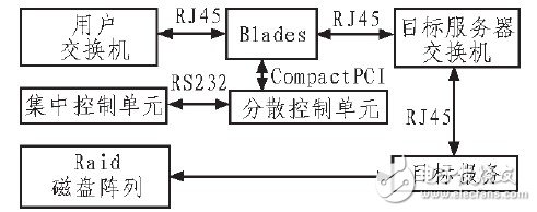
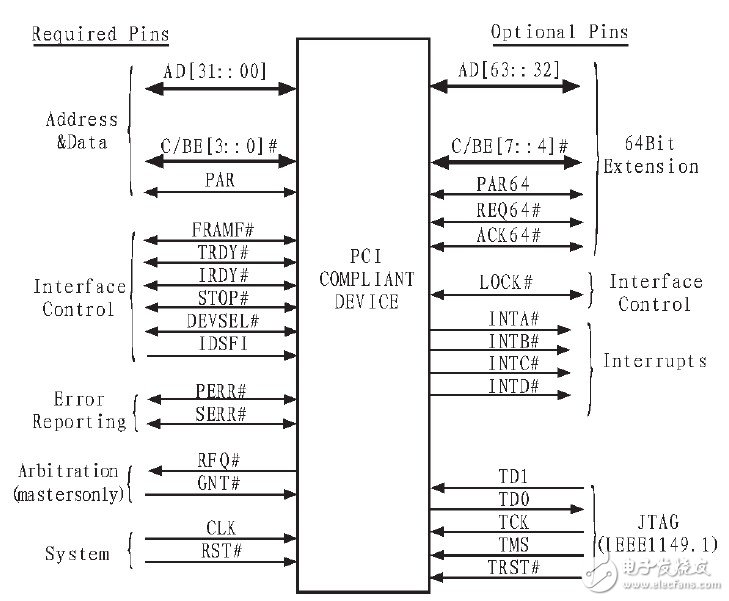
The next-generation rack server, Blade Server, uses the iSCSI protocol to implement network storage over TCP/IP, and uses Intemet to deliver SCSI packets anywhere on the planet. The blade server is a HAHD (High Availability High Density) low-cost server platform designed for specific application industries and high-density computer environments. Each blade is composed of "system server motherboard + control board", which can remotely start Windows NT/2000, Linux, Solaris and other operating systems. Similar to a standalone server, each blade can have no separate hard disk to store data, but multiple blades share a Raid disk array. In this mode, each blade runs its own system and serves different user groups specified by the user. There is no correlation between them. However, these blades can also be grouped into a server cluster through system software. In cluster mode, all Blades are connected to provide a high-speed network environment for resource sharing and service to the same user base. To increase overall performance, simply insert a new blade into the cluster. The blades are hot swappable for easy replacement and minimal maintenance time. Figure 1 Schematic diagram of the blade The location of the blade in a single rack system is shown in Figure 2. Figure 2 blade system structure In a single-rack system, the user switch and the Blade are connected through the Gigabit network interface of the RJ45. The user accesses the Blade server through the user switch for data exchange, and can be accessed by the Internet to the user switch from anywhere in the world. The centralized control unit has PC common output ports such as network ports; the distributed control unit (DMU) communicates with the Blade through CompactPCI; and communicates with the centralized control center (SMU) through the 232 serial port. The DMU and the SMU jointly complete the KVM switching and the acquisition of the Blade state function. The PCI bus is a local bus that does not depend on a specific processor. From the structural point of view, PCI is a first-level bus inserted between the CPU and the original system bus. The specific management of this layer is realized by a bridge circuit, and the interface between the upper and lower sides is realized to coordinate the data transmission. The manager provides signal buffering to support 10 peripherals and maintain high performance at high clock frequencies. The PCI bus also supports bus mastering technology, allowing smart devices to take control of the bus when needed to speed up data transfer. Figure 3 PCI local bus pin diagram Usually, the PC uses a local hard disk to boot the operating system and complete the device driver. The Blade starts the system through the network, so the network configuration is booted before the operating system, and initialization and driver loading are completed. In order to solve this difficulty, we use the "PCI + FPGA + Flash" structure to burn the initialization and drive loader of the dual-port Gigabit NIC PCI device in Flash. The CPU loads the program in Flash to the system memory when the system is powered on. . Since the data transmission is a PCI bus, and Flash is a standard data bus, there is a problem of data bus conversion. The solution to the problem is to complete the communication between the PCI device and the Flash through the FPGA. The following describes how to use the FPGA to complete the communication. Communication between the PCI interface and Flash. The whole FPGA system design is based on the PCI2.2 slave device design idea. The PCI master device is a PCI bridge chip. The FPGA is used to complete the PCI slave device function, and the terminal is a Flash chip. In the FPGA system, the design parameters of the PCI bus interface part are: PCI clock is 33 MHz (CLK), 32-bit I/O interface (AD[310]), and the terminal interface can provide 20-bit or 32-bit data lines. Communication between the PCI master device and the terminal flash is implemented using a PCI slave device (FPGA). In the logic design of the FPGA, the terminal is an abstract device that combines the memory space and the I/O space. In the actual design, the terminal Flash has only the corresponding memory space.
N-BK7 Precision Windows are ideally suited for industrial and low power laser applications. The high tolerance design yields minimal beam distortion and scatter. Broadband coating options extend the range of these precision windows through the visible and near-infrared spectra.
Our plane plates are also available with the following coatings: Bk7 Wafers,K9 Wafers,Thin Transparent Glass,4 Inch Bk7 Wafers Zoolied Inc. , https://www.zoolied.com
The author focuses on the internal architecture of the blade server and the introduction of the overall solution, mainly discusses the specific implementation method of PCI data exchange between the blade and the motherboard based on FPGA.
Servers (blades) in the rack can share multiple sets of keyboards, blades, and mice through a smart KVM converter board to access multiple servers (blades), making it easy to upgrade, maintain, and access files on the server. A single blade is connected to the main board through the PCI bus, and the transmission and exchange of the data in the blade are performed through the channel. The actual composition of the blade is as shown in FIG. 

Since each Blade does not have a separate hard disk, all Blades are booted remotely through the target server, and the configuration is completed and the operating system pre-installed in Raid is started, while DHCPD (dynamically assigned IP address), ADSS, iSCSI for each Blade allocates Raid disk array space. That is, each Blade starts the system through the network interface, so the network configuration must complete the initialization and drive loading before the operating system boots.
The general PCI2.2 interface signal is shown in Figure 3. In the left half of Figure 3 is the necessary signal and the optional signal is listed on the right. The "#" symbol on the right side of the signal name indicates that it is active low, and the "#" symbol is not active high. According to the function division of the signal, it can be divided into system signal group, address data group, interface control group, arbitration management group, error test group, interrupt function group, Cache support group and other functional groups. 
According to the module design idea of ​​FPGA, the whole system is designed by function in Verilog language. The output of each module can provide input for other functional modules. The functions and design ideas of each module are as follows:
The "PCI top-level module" is the top-level module of the system, which completes the definition of each enable switch of the system port and calls the other five functional modules.
The "Configuration Module" completes the setting of the PCI Slave Configuration Register.
The "base module" implements two functions: 1) configuring the base address of the I/O space and the memory space (memory space); 2) notifying the PCI slave state machine (The State Machine).
The "state machine module" is the core of the entire design and controls all data transfers from the PCI master to the terminal. In the PCI address transfer phase, it is determined whether to configure read/write, memory space read/write or I/O space read/write by sampling C/BE[30] and IDSEL.
The "verification module" performs parity check on the AD[310] and C/BE[30]# signals to ensure the validity of the data.
"Re-entry module" If the PCI slave device performs a read/write operation, it must enable DEVSEL within 6 clock cycles (defining the PCI slave device as slow=10 b, slow device). If the PCI slave device performs data transfer ( DEVSEL has been enabled. If the terminal does not enable READY# within 9 clock cycles, it will inform: "The State Machine module", the terminal temporarily suspends the current data transfer until the transfer condition is met, and then restarts the data transfer.
VIS range (ARB2: R < 0.5 % per surface, AOI = 0°, λ = 450 - 700 nm).
NIR range (ARB2: R < 0.5 % per surface, AOI = 0°, λ = 725 - 1050 nm).
Nd:YAG fundamental (ARHS: R < 0.2 % per surface, AOI = 0°, center wavelength 1064 nm)
Reflective aluminum coating (RAL: for λ = 400 nm - 12 μm, damage threshold > 200 mJ / cm2)
Front surface mirror silver coating (RAGV: for λ = 500 nm - 12 μm, damage threshold > 200 mJ / cm2)
For customized optics please contact our sales team for your individual quotation.