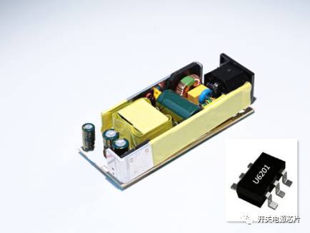
Switching power supply chips are beginning to play an increasingly important role in our lives, filling every corner of our lives, whether it is a charger for various digital products or an electronic product necessary for our lives. Let me introduce you to this old friend switching power chip today: The main circuit of the switching power supply is composed of input electromagnetic interference filter (EMI), rectification and filtering circuit, power conversion circuit, PWM control circuit and output rectification and filtering circuit. The auxiliary circuit has an input over-voltage protection circuit, an output over-voltage protection circuit, an output over-current protection circuit, and an output short-circuit protection circuit. 1 Lightning protection circuit: When there is lightning strike and high voltage is generated through the power grid, the circuit consists of MOV1, MOV2, MOV3: F1, F2, F3 and FDG1. When the voltage applied across the varistor exceeds its working voltage, its resistance decreases, so that the high-voltage energy is consumed on the varistor. If the current is too large, F1, F2, and F3 will burn and protect the latter circuit. 2 Input filter circuit: The double π-type filter network composed of C1, L1, C2 and C3 mainly suppresses the electromagnetic noise and clutter signals of the input power source to prevent interference to the power supply and also prevents high-frequency clutter generated by the power supply itself. Interference with the grid. When the power is turned on, the C5 should be charged. Because the instantaneous current is large, adding RT1 (thermistor) can effectively prevent the inrush current. Since the instantaneous energy is completely consumed on the RT1 resistor, the RT1 resistance decreases after the temperature rises after a certain time (RT1 is a negative temperature coefficient component), at which time the energy consumed is very small, and the latter circuit can work normally. 3 Rectifier filter circuit: After the AC voltage is rectified by BRG1, it is filtered by C5 to obtain a relatively pure DC voltage. If the C5 capacity becomes smaller, the output AC ripple will increase. 1. Working principle of MOS tube: At present, the most widely used insulated gate field effect transistor is MOSFET (MOS tube), which uses the electroacoustic effect of semiconductor surface to work. Also known as surface field effect devices. Since its gate is in a non-conducting state, the input resistance can be greatly improved up to 105 ohms. The MOS transistor uses the magnitude of the gate-source voltage to change the amount of induced charge on the semiconductor surface, thereby controlling the drain current. . 60W series 12V5A energy efficiency six-level solution ±5% constant voltage constant current accuracy, fast dynamic response control Standby power consumption is less than 75mW Automatic compensation of input voltage. Inductive inductance change Automatic compensation of input voltage. Inductive inductance change Ultra low starting current Harbour Marine Diesel Generator Harbour Marine Diesel Generator,Onshore Marine Generator,Offshore Marine Generator,Marine Engine Jiangsu Vantek Power Machinery Co., Ltd , https://www.vantekpower.com