Abstract: PCIe bus not only has a simple hardware interface, but the software and PCI bus are fully compatible, and the transmission speed is several ten times that of the PCI bus. Aiming at the demand of real-time video acquisition and recording of the carrier task system, an aviation video acquisition and recording system based on PCIe bus is designed. The codec of the video data stream and the design of the PCIe bridge interface are realized by the field programmable logic device (FPGA). Simplified hardware interface design and improved system efficiency. The practical application of the system in a certain type of digital confrontation training system shows that the design is practical and feasible. This article refers to the address: http:// Battery Anti-Theft System,Vibration Anti-Theft Function Battery,Gps Anti-Theft Function Battery,Monitoring On Computer And Phone Battery Wolong Electric Group Zhejiang Dengta Power Source Co.,Ltd , https://www.wldtbattery.com
Keywords: PCIe bus; video acquisition; hardware design language; INDS
0 Introduction The transmission of state data and control data between avionics systems is mainly because the amount of data is not very large and the transmission rate is not high. For example, the most popular airbus ARINC 429 and 1553B buses are at 100 kbps and 1 Mbps, respectively. With the improvement of flight training intensity and precision, multi-channel video images of flight test and training process need to be recorded in real time for post-mortem analysis and system design improvement. Compared with the transmission state control information, these video data are huge, and higher requirements are imposed on the mass storage and high-speed data transmission of the avionics system. This paper proposes a design scheme of aviation video acquisition and recording system, which adopts PCIe bus construction system with speed up to 2.5Gbps. PCIe bus has high-speed data transmission capability and good peripheral interface, which is beneficial to real-time of large-capacity signals. transmission. It effectively solves the real-time acquisition and recording of airborne multi-channel video data, and provides a convenient means for post-evaluation and performance analysis improvement of aviation training mission system.
1 System design In the aerial video acquisition and recording system, the camera frames the real-time picture video data of the carrier task system in a predetermined format and transmits it to the video acquisition module through the LVDS signal bus; the LVDS signal level is performed by the video acquisition module. After the conversion process, the single-ended video digital signal is sent to a programmable logic device (FPGA) for video decoding processing. The decoded digital video is directly sent to the monitor through the SAA7121 video encoder, allowing the pilot to grasp the training situation and effect in real time: on the other hand, the high-speed PCIe bus is transmitted to the embedded CPU module for video data compression storage for post-mortem analysis. . The overall structure of the aviation video acquisition and recording system is shown in Figure 1. 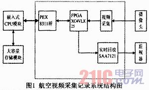
2 system hardware design The hardware design of the system is mainly focused on the circuit design of each functional module, which is the platform foundation of software design and system debugging. The hardware design should ensure the high reliability of the system operation, and under the premise of meeting the requirements, minimize the difficulty of designing and debugging the programmable logic and system software.
2.1 Video data acquisition Video data recorded by the camera is transmitted with LVDS differential level signal, and level signal conversion is required to perform subsequent video signal recording processing. The video data transmitted by the camera includes 4 pairs of LVDS differential signals, CLK+/CLK- is the clock for collecting data, and the remaining 3 pairs of differential signals contain pixel gray scale. The differential signal is converted by the DS90LV032 into four single-ended digital signals for later processing. The video acquisition circuit is shown in Figure 2. 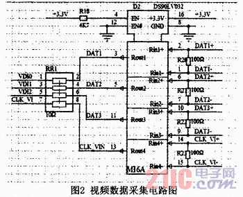
Because of the high frequency of the video data, the converted single-ended signal should be terminated with a 10 Ω resistor to suppress reflections and improve signal stability.
2.2 Video Decoding and Processing The video data collected by the front end must be processed to display and compress the memory in real time. Due to the large amount of video data, in order to achieve the smoothest and fast processing, data processing should be performed directly by hardware logic. The decoding and processing of video data is mainly done by FPGA, which is also the main task of programmable logic design.
The current DS90LV032 transmits the video data after the signal conversion to the FPGA, and the FPGA completes the decoding and restoration of the video signal, and the format conversion is synchronously transmitted to the CPU module for real-time recording and real-time playback of the video module. The hardware interface design of FPGA video data processing is shown in Figure 3. 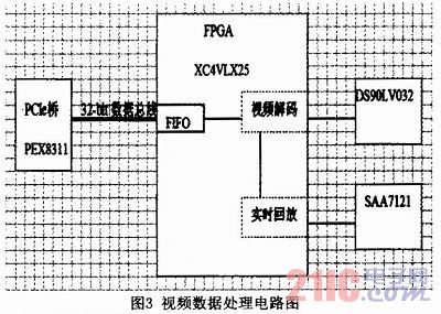
2.3 Video Data Playback Video playback is a convenient way for pilots to monitor training and testing in real time. The system uses Philips' SAA7121 video encoder to convert the processed video data from the FPGA into a PAL integrated video for display to the monitor in front of the pilot. As shown in Figure 4. 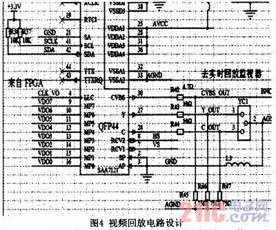
The SAA7121 needs to be initialized before it can work. Initialize the working mode by setting the register of the encoder. The initialization is done through the I2C bus, and the system's I2C bus interface is implemented by the FPGA. The synchronous clock CLK VO and 8-bit parallel video data are transmitted by the FPGA decoding process. The operating frequency of the encoder is 27MHz, and the decoded video data of the FPGA is sent to the monitor through the integrated video signal CVBS of the SAA7121 encoder. An alternate YC component video interface was also designed.
2.4 Video Transmission The captured video data needs to be transmitted to the embedded CPU through the PCIe bus after FPGA decoding processing to facilitate real-time compression storage. Achieving high-speed PCIe bus is the key to massive data transmission. The data transmission bus technology is a process of continuous updating and development. In the initial stage of data communication, serial communication has a wide range of applications due to its simple signal and convenient implementation. For example, RS422 serial communication is still very active despite its low speed. In order to solve the bottleneck problem of serial communication, the parallel transmission bus is adopted, and the rate of parallel communication depends on the clock frequency and the data width. At present, the most popular 33MHz/32bit PCI bus has a peak transmission rate of 132Mbps. As the clock frequency continues to increase, the data width of the parallel communication bus becomes an obstacle to continuing to increase the rate. Due to line crosstalk and feedback at very high frequencies, it is difficult to ensure the consistency of data synchronization of multiple parallel bus signals. The data transmission technology is parallelized to serial, and the parallel bidirectional PCI bus is developed into a serial one-way PCIe bus. . The PCIe bus with a rate of up to 2.5 Gbps has three pairs of differential signals, namely the synchronous clock CLK+/CLK-, the received signal R+/R-, and the transmitted signal T+/T-. The PCIe bus design circuit is shown in Figure 5. 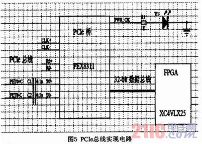
In the high-speed signal transmission bus of PCIe, data is not transmitted directly through the voltage signal of the signal conductor, but by high-frequency coupling. C1 and C2 in Figure 5 are the coupling capacitors of the transmitter and should be as close as possible to the bridge. Each pair of differential signals should have a coupling capacitor. The coupling capacitors for the clock and receive signal pairs in Figure 5 are implicit in the PCIe master.
3 system logic design Based on the hardware design, logic design becomes the key to the performance of the whole system. The logic design completes the timing control of the entire system, the acquisition and decoding of the video data stream, the encoding of the video playback, and the design of the PCIe bridge interface.
3.1 Video Decoding In the logic design, the function of video decoding is to decode the single-ended signal converted by DS90LV032 and write it to the FIFO buffer for processing by subsequent logic. The VHDL form of its logical interface is described as follows: 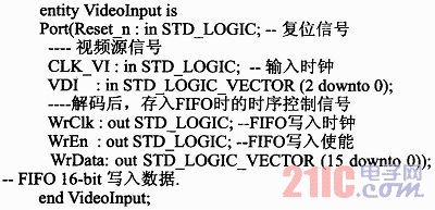
The camera acts as a video source and outputs a 3-bit data on each rising edge of CLK. In contrast, the decode logic latches a 3-bit data on the falling edge of CLK, performs a pipeline latch, and restores the grayscale data of the video. For a 16-bit data, a total of 6 times is required.
3.2 Video Encoding To support the SAA7121 encoder, the video playback logic includes an I2C interface and a PAL video encoding for initialization. The register of SAA7121 is 8-bit, then its I2C interface can be described as follows: 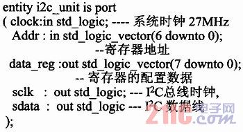
The upper logic calls this module, and each time it is called, a register is configured. The configuration data for all 128 registers is pre-customized and stored in a constant array.
The initialized SAA7121 works fine. At this point the logic should continuously deliver video data. Its logical interface can be described as follows: 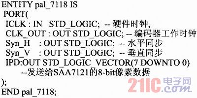
3.3 PCIe Bridge Interface Design Data high-speed transmission is mainly reflected in the actual throughput of the PCIe bus, which is the bottleneck of the decoded data transmission. The logic design must take into account the convenience and efficiency of the software. Interface logic design focuses on the burst mode of interrupt logic and data transfer.
The video data to be transmitted is first sent to a FIFO, the write end is 32k×16bit, and the read end is 16k×32bit. The write is suitable for the width of the video data, and the PCI32-bit bus is played during the read and transfer. The advantage of speeding up the conversion. The interrupt logic is designed as follows:
(1) When the write data reaches 1/4 of the FIFO capacity, that is, when the write is 4k×32bit, an interrupt is generated. This condition can be determined based on the programmable null of the FIFO, that is, when PRG1 Empty = '0'.
(2) When the host responds to the interrupt and starts reading the FIFO data, the interrupt is cancelled.
(3) After the end of this burst read, it is allowed to re-determine the interrupt condition according to the conditions.
The most important part of the logic design of the PCIe bridge interface is to provide seamless glue logic for its local bus, supporting PCIe single access and burst access. Its interface state machine is as follows: 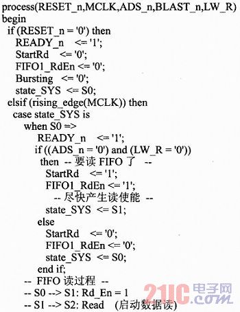
The local bus of the bridge is designed with a 50MHz clock. For a 32-bit data width, theoretically it can achieve a throughput of 200Mb/s. After the actual measurement of the application software, the rate of 143 Mb/s can be achieved. Considering the many overheads of the software, this rate has been ideal.
5 System Software Design The software design platform of the system adopts Windows XP Embedded. The software is divided into the driver and video compression and processing application for this hardware system. The application saves the video as a video format that can be played by a normal player. Each frame of video is 256 lines x 256 columns with a total of 64K pixels. In the driver software, when the device is turned on, apply a set of buffers, a total of 128 buffers. This buffer is transparent to the application, and each buffer can hold a complete video frame, as shown in Figure 6. There are two main threads in the driver, the interrupt thread and the data read thread.
In the logic design, whenever an interrupt is generated when 4kx32bi is written in the FIFO, the driver's interrupt thread reads at least 16kB at a time in response to the interrupt. When the interrupt response reads the FIFO data, do not use a software loop similar to for(;;). This strategy is a single access in hardware timing and is inefficient. Only DMA can trigger the burst cycle in the logic design to maximize hardware performance. When starting DMA, be sure to enable its burst bit operation length to be fixed to 16kB. Thus, each interrupt response becomes a pointer to maintain the current write buffer of the DMA, fill in the current write buffer address, and then start the DMA. 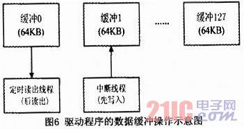
In the application, a timed thread is used to read the video data through the driver, and then compressed to store the video file in JPEG2000 format. The algorithm for periodically reading video data needs to be optimized, because if the data readout thread is too slow, the interrupted thread may overwrite the unread buffer when it is written, which may result in loss of data frames in the stored video, affecting the continuity of the recorded video. .
5 Conclusion In this paper, the combination of FPGA and embedded CPU large-capacity data storage is adopted. The real-time and reliability requirements of video data collection and recording are fully considered in all processing steps of the system. Airborne multi-channel real-time video data acquisition is designed. Record system. The system hardware is simple in design and can collect multiple video data at the same time. The application in a certain digital confrontation training evaluation system shows that the design scheme satisfies the expected index requirements and solves the key problems of multi-channel video data acquisition and real-time recording in the carrier mission system. In real-time video information collection and data recording applications It has good versatility and scalability.