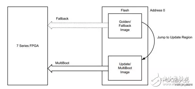
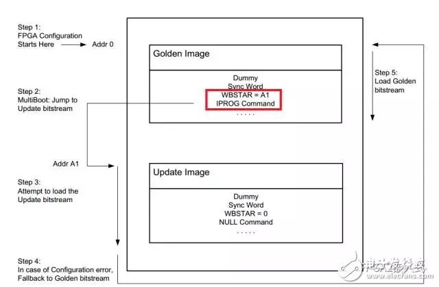
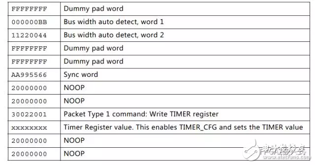
Nowadays, with the advancement of FPGA technology, performance improvement and cost reduction have been greatly improved, which makes the use of FPGA chips more and more extensive. Therefore, in order to reduce the cost of system maintenance and upgrade, we usually send the latest download files through the network, allowing users to directly download files to the FPGA for remote upgrade processing. However, once the download file is wrong, then the system is light and the function is wrong, but the direct crash does not work. In order to prevent this situation from causing significant impact or loss to users, Xilinx provides multiple configuration operations for FPGAs. FPGA multi-configuration allows for dynamic switching between multiple download files. When an error is detected during boot configuration, the FPGA triggers a fallback flag to ensure that a known good file can be loaded. The details are as shown below: In short, your .mcs file contains two or more download files, and then the address 0 starts to store an available download file (mostly the old one before the upgrade), the following address ( ADDR_1) stores the files you will be updating. When downloading, the FPGA will first read the updated file from ADDR_1. If an error occurs in this process, it will return to address 0 and read the previous file to ensure that the device still works. In addition to updating files, Xilinx's multi-configuration feature can also perform multi-tasking switch scheduling. Based on this function, as long as the Flash is large enough, it is possible to store multiple downloaded files. When the FPGA resource is small and the functions are independent and do not interfere with each other, sometimes the external control can be used to perform file switching download when different functions are required. For example, a device needs to perform four functions of ABCD, and ABCD is applied to different occasions, and there is no data exchange between them. If the FPGA resources can only implement one function or two in ABCD, then we can make four different bit files to implement the ABCD four functions and merge them into one .mcs file to download to Flash. When the A function is needed, we can use the button or the host computer to configure, let the FPGA load the A function download file to realize the A function. In the same way, this is also the case when only BCD is needed, which can greatly save FPGA resources. There is an ICAP core inside the FPGA that pre-configures the program load. The pre-configuration process can be processed in the .v code and the .bit file is generated accordingly. The default configuration if not processed by the code. The multi-configuration process of Xilinx FPGA is shown in the figure below. Please refer to the official document “xapp1247†for details. The available files are stored at the starting address of 0; the updated file is stored at the starting address of A1. After power-on, the FPGA enters the Flash 0 address and detects the WBSTAR and IPROG instructions in the configuration register (configured in .v). If the WBSTAR address points to A1 and the IPROG instruction is correct, the FPGA will jump to A1 to read and load the file. If the WBSTAR address at A1 is 0 and there is no IPROG instruction, the file here is loaded. If an error occurs while loading the update file, the FPGA will jump to address 0 and reload the file that is guaranteed to be available. The instruction list for IPROG is as follows: For the IPROG instruction configuration, it must be done in this order. Once the data is incorrect or the order is incorrect, the FPGA will not load the update file. In actual use, multiple loading of FPGAs is very helpful. Flexible use can avoid many on-site flaws and save a lot of cost for later technical support. The next section describes how to perform multiple configuration processing and use of code. Pcb Board,Circuit Board,Pcb Electronics,Custom Pcb Cixi Zhongyi Electronics Factory , https://www.cx-zhongyi.com