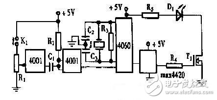
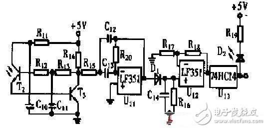
This paper introduces a high-reliability photoelectric switch (photoelectric sensor) circuit with frequency-stabilized modulated light to resist various interferences. It has high-power drive circuit and automatic gain control characteristics of phototransistor. The output stage of the detection circuit is equipped with Amplification and Schmidt hysteresis ensure high immunity to interference. It consists of two parts: a light-emitting circuit and a photoelectric receiving circuit. It has the advantages of anti-outer light interference, sensitivity without manual adjustment, stable and reliable operation, and can be applied in reflective or through-beam photoelectric switches. Illuminating circuit An LED driver circuit with a high power output that has the ability to emit 15 kHz modulated light. Figure 1 High-power driver for LEDs The first stage 4001 is a single pulse generator, which can output a detection pulse by manual button for fault repair. In order to stabilize the frequency of the modulated optical signal, the frequency divider CD4060 is used in the circuit. It has an external crystal oscillator with a multi-stage divider inside. For the 1M crystal, after a frequency division of 4 060, the square wave with a frequency stability of 151,625 kHz can be obtained, and then the current amplification of the power FET can simultaneously drive hundreds of LEDs to simultaneously emit light. Photoelectric switch receiving circuit with automatic gain control The infrared phototransistor T2 has a base lead. Therefore, sensitivity control can be performed thereon. The photocurrent of its emitter output is inverted by the amplifier tube T3 and fed back to the base of the phototransistor. Since there is a low-pass filter consisting of R13 and C11 in the feedback loop, this feedback is a negative feedback for the DC operating point and also allows the AC voltage gain to be controlled, which is the Automatic Gain Control (AGC) circuit. Figure 2 Photoelectric receiving circuit When the input optical signal is strong, the T3 collector signal has a strong tendency, which causes the DC operating point voltage of the base of the phototransistor T2 to decrease, thereby reducing the AC output of both T2 and T3. Therefore, this negative feedback system will make the AC output signal of T3 almost independent of the intensity of the light obtained by T2 over a wide range. It can be seen that when the input light changes, the T3 output signal does not change much. That is to say, the change in the distance between the light source and the phototransistor has little effect on the T3 output signal over a wide range. The output signal of T3 changes only after the light source is fully blocked. U11 forms a second-order bandpass filter that filters out signals other than 151,625 kHz. The gain of this stage is 1 and the Q value is 5, and the cutoff frequency, center frequency, and filtering characteristics are easily adjusted. Diode D1 and capacitor C14 form a detector circuit that demodulates the envelope signal from the 151625kHz signal. The above two parts of the circuit can filter out the effects of interference sources such as sunlight, fluorescent lamps, and incandescent lamps. The output circuit of Figure 2 consists of an amplifier stage U12 and a Schmitt circuit U13. The hysteresis effect of U13 can eliminate the critical jitter phenomenon of the photoelectric switch and avoid the false flip phenomenon of the photoelectric switch. Finally, the output state of the photoelectric switch is displayed by the light-emitting diode D2. Compute Stick Intel,Mini All In One Pc,Desktop Computer Mini Fan,Mini Pc Box Desktop C&Q Technology (Guangzhou) Co.,Ltd. , https://www.gzcqteq.com
